Download
1 / 24
250 likes | 533 Views
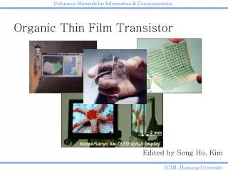
Towards Predictable Compact Model Descriptions for Organic Thin-Film Transistors. S. Mijalković , D. Green, A. Nejim Silvaco Technology Centre, St Ives, Cambridgeshire, UK A. Rankov , E. Smith, T. Kugler , C. Newsome, J. Halls Cambridge Display Technologies, Godmanchester , UK. e-nose.

E N D
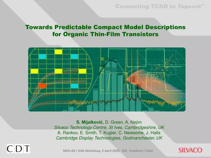
Towards Predictable Compact Model Descriptions for Organic Thin-Film Transistors S. Mijalković, D. Green, A. Nejim Silvaco Technology Centre, St Ives, Cambridgeshire, UK A. Rankov, E. Smith, T. Kugler, C. Newsome, J. Halls Cambridge Display Technologies, Godmanchester, UK MOS-AK / GSA Workshop, 3 April 2009, IHP, Frankfurt / Oder
e-nose e-skin Flexibledisplay Smart fabrics Organic Electronics:“Harry Potter’’ and “Star Trek” Technologies are Coming your Way! • Fast development of organic electronics is supported by applications that require low cost electronic circuits covering mechanically flexible large areas. • These include e-skin, e-paper, e-nose, smart-fabrics, flexible displays, printed electronics or radio frequency identification tags (RFID). Organic Solar Cells Organic Solar Cells • Organic electronics can be fabricated using faster and cheaper low temperature processes. • Basis of the future organic electronic circuits are organic TFTs (OTFTs). MOS-AK / GSA Workshop, 3 April 2009, IHP, Frankfurt / Oder
Organic Electronics: Forecast and Opportunities • The organic electronics will be a $30 billion business in 2015 mainly due to logic, displays and lighting. • It will be a $250 billion business in 2025, with at least ten billion dollars sales from logic/memory, OLED displays for electronic products, OLED billboard, signage etc, non-emissive organic displays, OLED lighting, batteries and photo-voltaics, with sensors almost at that level. • Organic lighting will severely dent sales of both incandescent and fluorescent lighting in the second decade from now. • Organic electronics in the form of electronic billboards, posters, signage and electronic books will revolutionize the conventional printing and publishing industry. • The future organic market will be newly created without replacing much from the inorganic semiconductors in existing electronics products. MOS-AK / GSA Workshop, 3 April 2009, IHP, Frankfurt / Oder
Organic Electronics:Challenge for Electronic Design Automation (EDA) • Inorganic semiconductor industry relies extensively on EDA software to support the iterative cycles of process, device and circuit technology improvements. • To further develop organic electronics industry, equivalent design tools are needed. • EDA tools essentially depend on numerical and analytical device models which are, in case of OSCs, not yet matured and quite sparsely implemented in commercial EDA tools. • Cambridge Display Technology (CDT) and Silvaco Europe have joined forces together in a TSB funded project entitled PMOS to enhance EDA tools for use in the organic electronics and to help move organic transistor technology from the labto the shop floor. MOS-AK / GSA Workshop, 3 April 2009, IHP, Frankfurt / Oder
UK Technology Strategy Board (TSB) Project: Physical Modelling of Organic Semiconductors (PMOS) Project partners • Cambridge Display Technology (CDT) • Expert in polymer light emitting diode (PLED) technologies. • Leader in development of solution processable (printable) organic. semiconductors for display fabrication. • Expertise in development of PLED materials and deposition processes. • Silvaco • Leading provider of TCAD and EDA software for IC design • Provides established products for TCAD process and device simulation, spice parameter extraction, circuit simulation, custom IC design and verification. Project activities • Design of OTFT devices using physical TCAD modelling. • OTFT spice modelling and parameter extraction. • Measurements and modelling of device reliability and aging effects. • The focus is on display device (OLED) drivers as these will be the first large scale organic semiconductor products. MOS-AK / GSA Workshop, 3 April 2009, IHP, Frankfurt / Oder
OFET Architectures and Peculiar Features • OSC morphology varies from amorphous to (poly)-crystalline. • OFETs are commonly realized using an OSC layer without a deliberate doping. • The carriers that contribute to the charge distribution and transport in OFETs must be injected from the metallic contacts. • Without particular semiconductor type of the OSC layer, OFET can operate in the electron or hole carrier accumulation mode depending on polarity of the gate voltage and capabilities of the contacts to inject particular carrier type. • The source and drain have no junction isolation. A drain/source leakage current is limited by intrinsic OSC conductivity and contact resistance rather then reverse junction current. • Contact resistances often dominate the OFET performance and represent a bottleneck to achieve full potential of the intrinsic transistor effect. • OFETs are typically characterized with much lower carrier intrinsic carrier mobility having different bias physical origin then their inorganic counterparts. MOS-AK / GSA Workshop, 3 April 2009, IHP, Frankfurt / Oder
Density of States and Carrier Concentration E E LUMO CB TRAPS VB HOMO Intrinsic DOS from molecular LUMO (HOMO) energy levels ranging from delocalized conduction and valence bands in molecular crystals to localized trap-like energy distributions amorphous OSCs. DOS from localized in-gap trap energy levels. MOS-AK / GSA Workshop, 3 April 2009, IHP, Frankfurt / Oder
Silvaco Atlas: OFET Example MOS-AK / GSA Workshop, 3 April 2009, IHP, Frankfurt / Oder
Variable Range Hopping Conductivity ModelPercolation Theory MOS-AK / GSA Workshop, 3 April 2009, IHP, Frankfurt / Oder
Sheet Channel Conductivity Exponential DOS distribution Carrier concentration Local channel conductivity Vissenberg and Matters, Phys. Rev. B, 1998. MOS-AK / GSA Workshop, 3 April 2009, IHP, Frankfurt / Oder
Sheet Channel Conductivity (and Mobility) Exact Model MOS-AK / GSA Workshop, 3 April 2009, IHP, Frankfurt / Oder
Channel Sheet Charge: Surface Potential (SP) Model Exponential DOS carrier concentration gives SP equation in accumulation operation mode: There is an approximate analytical solution (Gildenblat, et al., IEEE J. SSC, 2004) MOS-AK / GSA Workshop, 3 April 2009, IHP, Frankfurt / Oder
Channel Sheet Charge: Unified Charge Control Model (UCCM) MOS-AK / GSA Workshop, 3 April 2009, IHP, Frankfurt / Oder
Intrinsic Drain-Source Current Surface-Potential Based Model Charge Based Model MOS-AK / GSA Workshop, 3 April 2009, IHP, Frankfurt / Oder
Parameter Extraction in UTMOST IV MOS-AK / GSA Workshop, 3 April 2009, IHP, Frankfurt / Oder
Model Verification: Surface Potential Based Comparison between simulated (lines) and measured (circles and squares) output characteristics of the OTFT Comparison between simulated (lines) and measured (circles and squares) transfer characteristics of the OTFT MOS-AK / GSA Workshop, 3 April 2009, IHP, Frankfurt / Oder
Model Verification: Charge Based Comparison between simulated (lines) and measured (circles) output characteristics of the OTFT for Vg=-10V, -20V, -30V and -40V. Comparison between simulated (lines) and measured (circles) transfer characteristics of the OTFT in the linear operation region with Vds=-3V (blue line and circles) and saturation operation region with Vds=-30V (red line and circles) MOS-AK / GSA Workshop, 3 April 2009, IHP, Frankfurt / Oder
Model Verification: Temperature Variations Comparison between simulated (lines) and measured (circles) transfer characteristics of the OTFT in the saturation operation region at different temperatures: T=270K (dark blue) T=280K (light blue) T=300K (green) T=310K (pink) T=330K (red) MOS-AK / GSA Workshop, 3 April 2009, IHP, Frankfurt / Oder
Origin of Contact Resistance Surface Contamination Geometric • Top gate, bottom contact has greater area for injection, thus our preferred architecture • Oxide layer will grow on many metals • Residues from resist processes etc G Contamination layer Oxide layer S S G Top Gate Bottom Gate Morphology Electronic • Electronic barriers to injection into air stable, deep HOMO OSC LUMO • Voids in OSC to source/drain lead to poor contact • Crystal orientation important WF S HOMO MOS-AK / GSA Workshop, 3 April 2009, IHP, Frankfurt / Oder
Strong Influence of the Series Resistances MOS-AK / GSA Workshop, 3 April 2009, IHP, Frankfurt / Oder
Contact Resistance Extraction Contact resistance at L=0 500um Vg = -20V Vg = -30V Total Channel Resistance Vg = -40V Channel Length, L MOS-AK / GSA Workshop, 3 April 2009, IHP, Frankfurt / Oder
Non-Quasi-Static Effects MOS-AK / GSA Workshop, 3 April 2009, IHP, Frankfurt / Oder
Some Other Open Issues • Influence of the bias dependent bulk and interface traps:- extended surface potential equation including forward and reverse, (accumulation and depletion) operation mode,- a bias modulated back channel conductivity. • Leakage currents- bulk and contact limited leakage effect, - temperature dependence. • Short channel effects: - physics based channel length modulation,- effects of the depletion and strong lateral electric field on the drain side,- space-charge limited transport. • Gate leakage current model. • The influence of the OSC film thickness on the interface electric field - layered distribution of the accumulated charge due to the elongated molecular geometry and regular assembly,- floating body potential. • Aging and hysteresis of the OTFT characteristics within the model and the corresponding circuit design. MOS-AK / GSA Workshop, 3 April 2009, IHP, Frankfurt / Oder
Acknowledgement This work is supported by the UK Technology Strategy Board through the PMOS project TP/J2519J. We want to thank Prof. Benjamin Iñiguez and his group for valuable recommendations regarding compact organic TFT modelling.