Download
1 / 5
170 likes | 377 Views
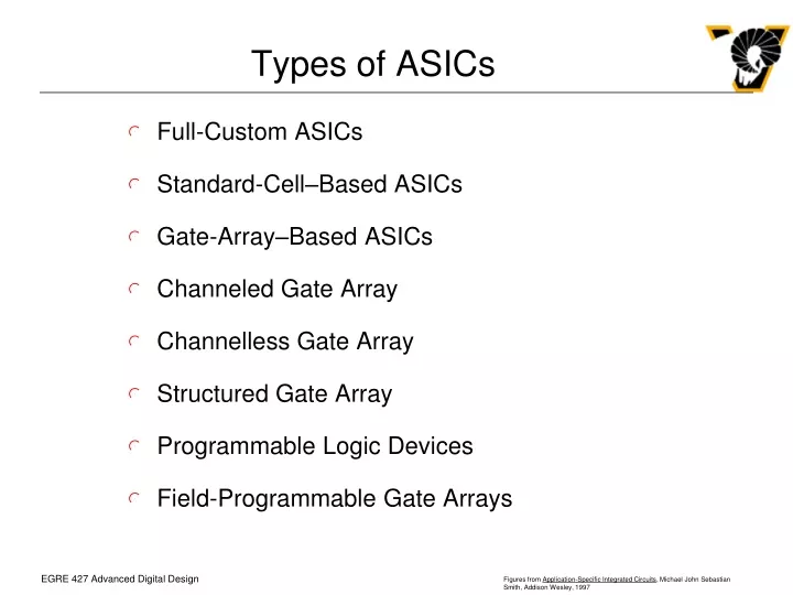
Types of ASICs. Full-Custom ASICs Standard-Cell–Based ASICs Gate-Array–Based ASICs Channeled Gate Array Channelless Gate Array Structured Gate Array Programmable Logic Devices Field-Programmable Gate Arrays. Gate-Array-Based ASICs.

E N D
Types of ASICs • Full-Custom ASICs • Standard-Cell–Based ASICs • Gate-Array–Based ASICs • Channeled Gate Array • Channelless Gate Array • Structured Gate Array • Programmable Logic Devices • Field-Programmable Gate Arrays
Gate-Array-Based ASICs • In a gate-array-based ASIC, the transistors are predefined on the silicon wafer • The predefined pattern of transistors is called the base array • The smallest element that is replicated to make the base array is called the base or primitive cell • The top level interconnect between the transistors is defined by the designer in custom masks - Masked Gate Array (MGA) • Design is performed by connecting predesigned and characterized logic cells from a library (macros) • After validation, automatic placement and routing are typically used to convert the macro-based design into a layout on the ASIC using primitive cells • Types of MGAs: • Channeled Gate Array • Channelless Gate Array • Structured Gate Array
Gate-Array-Based ASICs • Channeled Gate Array • Only the interconnect is customized • The interconnect uses predefined spaces between rows of base cells • Manufacturing lead time is between two days and two weeks Figure 1.5 Channel gate-array die • Channelless Gate Array • There are no predefined areas set aside for routing - routing is over the top of the gate-array devices • Achievable logic density is higher than for channeled gate arrays • Manufacturing lead time is between two days and two weeks Figure 1.6 Sea-Of-Gates (SOG) array die
Gate-Array-Based ASICs (cont.) • Structured Gate Array • Only the interconnect is customized • Custom blocks (the same for each design) can be embedded • These can be complete blocks such as a processor or memory array, or • An array of different base cells better suited to implementing a specific function • Manufacturing lead time is between two days and two weeks. Figure 1.7 Gate array die with embedded block
Gate-Array-Based ASICs (cont.) • Programmable Logic Devices • No customized mask layers or logic cells • Fast design turnaround • A single large block of programmable interconnect • Erasable PLD (EPLD) • Mask-programmed PLD • A matrix of logic macrocells that usually consist of programmable array logic followed by a flip-flop or latch Figure 1.8 Programmable Logic Device (PLD) die • Field Programmable Gate Array • None of the mask layers are customized • A method for programming the basic logic cells and the interconnect • The core is a regular array of programmable basic logic cells that can implement combinational as well as sequential logic (flip-flops) • A matrix of programmable interconnect surrounds the basic logic cells • Programmable I/O cells surround the core • Design turnaround is a few hours Figure 1.9 Field-Programmable Gate Array (FPGA) die