Download
1 / 75
1.12k likes | 1.92k Views
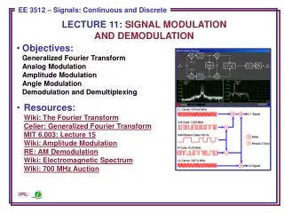
MODULATION AND DEMODULATION. Modulation – It is the process of changing one or more properties ( Amplitude, frequency or phase) of the analog carrier in proportion with the information signal. It is impractical to propagate information as it is over standard transmission media.

E N D
MODULATION AND DEMODULATION BDG(xx)
Modulation – • It is the process of changing one or more properties ( Amplitude, frequency or phase) of the analog carrier in proportion with the information signal. • It is impractical to propagate information as it is over standard transmission media. • Reverse process of modulation and converting the modulated carrier back to the original information is known as demodulation. BDG(xx)
Why Modulation is necessary? – • 1. It is difficult to radiate LF signal from antenna in the form of EM energy. • 2. Information signal often occupy the same frequency band that would interfere with each other. • (Channel is a specific band of frequencies allocated to a particular service.) BDG(xx)
Types of Modulation – • 1. Analog Modulation – (a) Amplitude Modulation (AM) – If information signal is analog and amplitude of the carrier is varied proportional to amplitude information signal, AM is produced. (b) Frequency Modulation (FM) – If frequency of carrier signal is varied proportional to information signal, FM is produced. (c) Phase Modulation (PM) –If phase of carrier is varied proportional to amplitude of information signal, PM is produced. BDG(xx)
2. Digital Modulation –(a) If the information signal is digital and amplitude of carrier is varied proportional to information signal, a digitally modulated signal known as Amplitude Shift Keying (ASK) is produced. (b) If frequency of the carrier is varied, Frequency shift Keying (FSK) is produced. (c) If phase of the carrier is varied , Phase Shift Keying (PSK) is produced. • If both Amplitude and Phase are varied proportional to the information signal, Quadrature Amplitude Modulation QAM is produced. BDG(xx)
Amplitude Modulation – It is a method of changing the amplitude of relatively high frequency carrier ( normally sinusoidal wave) in proportion with instantaneous value of modulating signal. • It is to be noted that the carrier frequency remains same and only amplitude varies. • Let em represents the modulating signal. em = Em sin ωm t and carrier signal is ec = Ec sin ωc t • Here Em & Ec – max. amplitude of modulating and carrier signal and ωm & ωc – frequency of modulating and carrier signal. BDG(xx)
A mathematical expression for modulated wave will be Eam = Ec + em = Ec + Em sin ωm t. • The instantaneous value of the amplitude modulated wave can be e(am) = Eam sin ωc t e(am) = (Ec + Em sin ωm t) sin ωc t . (##B4) • Modulation Index and Percentage Modulation – • Modulation Index m = Em/Ec. Term used to describe the amount of amplitude change in AM. • Should be always less than 1 to avoid any distortion.(known as under modulation) • m = 1 known as critical modulation. • m > 1 known as over modulation. ### BDG(xx)
AM power distribution- • Total power of AM wave is Ptotal = Pc +Pusb + Plsb =E^2car/R +E^2usb/R +E^2lasb/R, where R is characteristics impedance of antenna and E is RMS voltages. • Carrier power Pc = E^2carr/R = E^2c/2R • Psb = E^2sb/R , Esb = (mEc/2) / √2. = m^2 * E^2c/8R. P total =E^2c/2R* {1+m^2/2) = Pc{1+m^2/2} Ptotal/Pc = 1+m^2/2. BDG(xx)
Frequency Spectrum and Bandwidth – • The modulated carrier has new signals at different frequencies called sidebands or side frequencies, known as upper and lower sidebands. • f(lower sideband) = fc – fm • F(upper sideband) = fc + fm. • ### BDG(xx)
Am Modulator Circuits – • Two types- • 1. Low level modulation – modulation takes place at low carrier amplitude level. The modulated carrier is then amplified and transmitted. • 2. High level modulation - The carrier is amplified fully, then modulation takes place. Modulator has to operate at high power level. The modulated signal is then transmitted directly. BDG(xx)
Advantages and disadvantages of High and low level modulation – • High Level - • Advantages – Power efficiency is practically more than 80% and all the preceding linear amplifiers operate at low power level. • Disadvantages – • Requires high amplitude of modulating signal. Amplifier is non linear and hence generates intermodulation frequency components (Harmonics.) BDG(xx)
Low level – • Advantages – Less power consumption in the modulator as it operates at low voltage. • Being a class “A” amplifier, circuit is very simple. • Disadvantages – Modulator operates in class A, hence power efficiency is very low. BDG(xx)
Antenna Audio Amplifier Modulator PA Audio Input • AM High Level Transmitters - Antenna matching network. Mod class C AMP Driver Amp. Buffer AMP Crystal Osc. BDG(xx)
Carrier generation is by crystal oscillator. • Buffer and driver amplifiers brings power level of carrier to desired level and given to C class modulator amplifier. • Modulating signal is amplified by audio and audio power amplifier at a level suitable for modulation. • Modulating amplifier modulates carrier according to the modulating signal. • Output of modulator is fed to antenna via matching network, consisting of LC circuit in collector circuit of modulating amplifier. BDG(xx)
Antenna Audio Amplifier Modulator PA Audio Input • AM low Level Transmitters - Antenna matching network. Linear Class B Power Amp. Mod class C AMP Driver Amp. Buffer AMP Crystal Osc. BDG(xx)
A linear class B PA is used, for power amplification and amplified signal is fed to antenna. • Modulator amplifier performs modulation at relatively low power level and modulated AM signal is amplified by class B power amplifier to avoid distortion in the out put. BDG(xx)
AM Broadcast Transmitter – • Crystal osc generates carrier frequency signal. • Power level of carrier is raised by buffer amplifier. • Driver stage C class modulator is for partial modulation and further modulated by power amplifier. • Advantages- 1. If one or more components in main amplifier fails, driver stage still provides modulated output for transmission. Thus total shut down is avoided. BDG(xx)
2. Distribution of total power in driver and main amplifier. • The modulating signal is amplified and fed to modulator driver amplifier. • The modulating signal is coupled to class C driver and modulator through transformer coupling. • Part of transmitted signal is demodulated by the linear detector and given as negative feedback to audio amplifier to linearize the modulation chracteristics. BDG(xx)
DSB-SC and SSB-SC Amplitude Modulation – • In AM, information is contained in two side bands and not in carrier. Hence most of the energy is wasted. • In suppressed carrier system, carrier is not transmitted but only sidebands are transmitted, thus saving lot of transmitter power. BDG(xx)
DSB-SC Modulator – Product Modulator – • Modulating DSB-SC Signal Signal f(t) Carrier cos ωc.t Product Modulator F(t )cosωc.t BDG(xx)
By modulation theorem, the frequency spectrum of f(t) cos ωct will be • f(t) cos ωct FT ½{F(ω + ωc) +F (ω – ωc)} • Above equation shows two components – 1/2F(ω+ ωc) and 1/2F(ω- ωc) which are termed as sidebands and are located at + ωc and – ωc. • BW of each sideband is 2 ωm. • ### BDG(xx)
Balanced Modulator using Diodes (Ring)- • Refer circuit diagram- • Let modulating input is zero initially. • In the positive half cycle of carrier signal, D1 & D2 are forward biased and D3&D4 are reversed biased. • Due to center tapping of T2, current is equally divided in upper and lower portion of primary winding. • Hence the magnetic field produced by upper and lower winding are equal but opposite and hence output is zero. BDG(xx)
When a sinusoidal modulating signal is applied to the primary of T1, which appears at secondary of T1. • In the positive half cycle, D1 and D2 are forward biased connecting secondary of T1 to primary of T2. • In the negative half cycle, D3 and D4 are forward biased connecting secondary of T1 to primary of T2. When D3 & D4 conduct, the polarity of the signal is opposite to that of modulating signal. • Thus carrier is totally supressed. BDG(xx)
Balanced Modulator using FETs – (##) • The carrier signal is applied to the center tap of secondary of T1 from primary of T2 and output is from T3. • The signal is applied to two gates of FETs in phase through the secondary of T2. • Modulating signal appears out of phase (180 degrees) at the gates . • If there is no modulating signal, FET current due to carrier is equal and opposite in direction and no out put is produced at the secondary of T3, thus carrier is suppressed. BDG(xx)
When modulating signal is applied, currents id1 and id2 flows in the primary of T3. • Since modulating signal is applied 180 degrees out of phase at the gates of FETs, the FET currents due to modulating signal are equal but not opposite and hence do not cancel each other. • Hence output produced at the secondary of the transformerT3 is DSB out put produced by FET balanced modulator. • To prove that BM produces DSB Out put?(##) BDG(xx)
Switching Modulator –(##) • In this type of modulator, multiplication is replaced by simple switching operation. • Diode is assumed to act as a ideal switch i.e. it presents zero impedance in forward biased condition and infinite impedance in reverse biased condition. • The diode switch is controlled by carrier c(t). • When c(t) is more than zero, diode is forward biased and reverse biased when c(t) is less than zero. • Ec>>Em. BDG(xx)
Single Side Band – Suppressed Carrier (SSB-SC) • We have studied techniques of suppressing carrier. • Now let us study techniques of suppressing one sideband. • These techniques are (i) Filter Method (ii) Phase shift method, BDG(xx)
Linear Amplifier • Filter method to generate SSB – SB suppression filter Carrier Signal Balanced Modulator Balanced Mixer Crystal Osc. Modulating Signal BDG(xx)
Balanced modulator produces DSB output containing both the sidebands. • It is given to sideband suppressing filter to remove unwanted sideband. • Filter must have a flat passband and extremely high attenuation outside the passband. • To get this type of response the Q of the tuned circuits must be very high. • Required value of Q factor increases as the difference between modulating frequency and carrier frequency increases. BDG(xx)
SSB suppression filter suppresses one of the sidebands • Frequency of the SSB signal at the output of the filter is very low as compared to the transmitter frequency. • Hence the frequency is boosted up to the transmitter frequency by the balanced modulator and crystal oscillator. ( up conversion). • SSB signal is then amplified by the linear amplifiers. BDG(xx)
Modulating Signal Balanced Modulator M1 • Phase Shift Method to generate SSB - 90 degrees Phase Shifter Linear Power Amplifier 90 degrees Phase Shifter Summing Amplifier Carrier Generator Balanced Modulator M2 BDG(xx)
The carrier signal is shifted by 90 degrees and applied to M1. • Modulating signal is directly applied to M1. • Carrier signal is directly applied to M2. • Modulating signal is phase shifted & applied to M2. • Both modulators produce an output consisting of only sidebands. • M1 generates USB and LSB but each one is shifted by +90 degrees. • M2 generates USB shifted by +90 and LSB shifted by - 90 degrees. BDG(xx)
The outputs of the BM are added in summing amplifier. • Since USBs of both BMs are phase shifted by +90 they are in phase and add to produce double amplitude signal. • But LSBs of BM are (+90 and -90) 180 degrees out of phase and hence cancels each other, giving only USB SSB signal. • Carrier is suppressed by BM. • Let us prove this mathematically. • ## BDG(xx)
Synchronous Detection of DSB SC Signal – • DSB- SC signal can be detected by synchronous detector. f(t) cosωc t Multiplier LPF 1/2f(t) Carrier cosωc t BDG(xx)
The modulated signal f(t) cosωct is given to the multiplier. • The modulated signal is multiplied with locally generated carrier cosωc t. • Multiplier output signal is f(t) cos^2. ωct. • ### • LPF has cutoff frequency just more than that ωm. Hence passes the signal 1/2f(t). • Since 2 ωc >> ωm, the signal 1/2f(t) cos2ωct is not passed by LPF. • So output is fo(t) = 1/2f(t). BDG(xx)
Synchronous Detection of SSB SC Signal – • Synchronous detector – SSB Signal essb(t) Multiplier LPF Output 1/2f(t) Carrier cosωct BDG(xx)
Advantages of DSB-SC and SSB- SC – • 1.BW is reduced hence more number of channels can be transmitted in same available BW. • 2. As the carrier is suppressed the power requirement is also reduced. • 3. Noise is reduced as BW is reduced. • Disadvantages of DSB-SC and SSB- SC – • 1. Complicated process. • 2. High quality filters with good stability and selectivity are required for narrow BW operation. BDG(xx)
Amplitude Modulation by multiple sine waves - • In reality, modulation takes place due to multiple modulating waves. • Hence consider what will happen if two or more sine waves modulate carrier simultaneously. ## BDG(xx)
AM Receiver with double conversion – • In superheterodyne receivers, Intermediate Frequency (IF) is used for amplification and uniform gain. • For stability of IF amplifier, the IF shall be as low as possible. • For good image frequency rejection IF shall be as high as possible. • To achieve these two extreme requirements, two IFs can be used, first high IF for image frequency rejection and second low IF for stable amplification. . BDG(xx)
Antenna • Double conversion AM Receiver - 1st IF Conv. 2nd IF Conv. AM Detector RF Amp. 2nd IF Amp. 1st LO 2nd LO BDG(xx)
Signal received from antenna is passed through RF amplifier to increase amplitude of received signal and to improve signal to noise ratio. • Then signal is passed through 1st IF convertor, to generate IF of 10.625Mhz. This enable us to push image frequency (IF x 2) away from RF range. • First IF is then converted to 2nd IF of 455khz, passed through IF amplifier and then to detector. BDG(xx)
Advantages – 1. Easy amplification • 2. Better image frequency rejection. • Disadvantages – 1. Critical design of first conversion stage. 2. Additional stage of IF conversion. BDG(xx)
Vestigial Sideband Transmission – • SSB works satisfactorily for an information bearing signal(speech signal) with energy gap around zero frequency. • But for transmission of wideband signals, we have to look to a new method of modulation for two reasons. • 1. The spectra of wideband signal contain significant low frequencies, which makes it impractical to use SSB modulation. • 2. The spectral characteristic of wideband data befit the use of DSB-SC. But DSB-SC requires a transmission BW equal to twice the message BW, which violates the BW conservation requirements. BDG(xx)
To overcome these limitations, we need a compromise method of modulation that lies between SSB and DSB-SC in its spectral characteristics. • Vestigial sideband (VSB) is that compromise scheme. • VSB modulation distinguishes itself from SSB modulation in two practical aspects – • 1. Instead of completely removing a sideband, a trace or vestige of that sideband is transmitted, hence the name “vestigial sideband” BDG(xx)
Instead of transmitting the other sideband in full, almost the whole of this second band is also transmitted. • Transmitting BW of a VSB modulated signal is defined as BT =fv + W, where fv is the vestige BW and W is the message BW. • Typically fv is 25% of W which means that the VSB BW BT lies between the SSB BW ‘W’ and DSB – SC BW 2W. BDG(xx)
Generation of VSB using filter method- Product Modulator BP filter H(f) VSB signal s(t) Message signal m(t) Carrier Ac cos(2*pi*f*t) BDG(xx)
The BP filter is designed in such a way that it is suppresses one side band partially and passes a portion (vestige) of other sideband. • Output of BP filter is VSB signal. • Magnitude Response of VSB Filter - ## • Advantages of VSB -1.equencies near fc are transmitted without any attenuation. 2. BW is reduced as compared to DSB. • VSB is mainly used for TV transmission. BDG(xx)
Generation of VSB using Phase discrimination Method – • Principle of this method will become easy to understand once we determine the time domain description of the VSB wave. ### • Demodulation of VSB – Input VSB signal s(t), output signal v0(t), Product modulator output is v(t). ### Input Product modulator LPF Output A’ccos 2*pi*fc*t BDG(xx)