Download
1 / 17
250 likes | 474 Views
Manufacturing Processes. Micro Fabrication. Associate Professor Su-Jin Kim School of Mechanical Engineering Gyeongsang National University. Index. Micro fabrication of IC(Integrated Circuits) 반도체제조 Weiper( 웨이퍼 ) Lithography( 노광 ) Etching( 식각 ) Doping( 확산 ) Deposition( 증착 )

E N D
Manufacturing Processes Micro Fabrication Associate Professor Su-Jin Kim School of Mechanical Engineering Gyeongsang National University
Index • Micro fabrication of IC(Integrated Circuits) 반도체제조 • Weiper(웨이퍼) • Lithography(노광) • Etching(식각) • Doping(확산) • Deposition(증착) • Packaging(포장) • MEMS(Microelectromechanical system) 미소기전
Micro-manufacturing • Manufacturing on a microscopic scale • IC: Integrated circuit • MEMS: micro electro mechanical system • Products • Sensors • Inkjet printing heads • Micro-actuators • Hard-drive heads • Computer processors • Memory chips
Transistor to IC • Transistors(1947) IC (integrated circuits), MOS (metal-oxide-semiconductor) VLSI (very large-scale integration) • Moore’s Law : The number of transistors per chip doubles every 18 months. 1st Transistor IC
Clean Rooms • Essential for the production of IC (integrated circuits). • Cleanliness are defined by class of the clean rooms. • Air is passed through a high-performance particulate air (HEPA) filter. • Largest source of contaminants is people.
- Si - - - - - B P - - - - - - Silicon (Semiconductors) • Natural silicon dioxide SiO2 is an excellent insulator. • Single crystal silicon Si is semiconductor. • Get n-type by dopingP or p-type doping B. +phosphorus +boron SiO2 Insulator Single crystal silicon n-type p-type
Integrated Circuits; IC Process Ingot Wafer Wafers Coat photoresist Photolithography Remove exposed photoresist Lithography Wet etching Dry etching Etching Diffusion Ion implantation Doping Film deposition Oxidation Deposition Wire bonding Packaging Device 1967: http://www.youtube.com/watch?v=z47Gv2cdFtA (30min)
Ingot & Wafer • natural SiO2 purification electric-grade silicon Si • Single-crystal silicon ingot is grown from the purified silicon melt. • The Ingot is cut into silicon wafers. The wafers are polished until they have mirror-smooth surfaces. Wafer: http://www.youtube.com/watch?v=LWfCqpJzJYM&feature=related
Lithography • Drop down photoresist on spinning wafer. • Photolithography : UV light passes through mask to wafer surface. • Exposed photoresist is dissolved by a solvent. Photolithography: http://www.youtube.com/watch?v=9x3Lh1ZfggM&feature=related
Etching 식각 • The photoresist protects material not be etched away in an acid solution. • After the etching the photoresist is removed and the desired shape becomes visible. scale: transistor level (~50-200nm) IC Process: Photoresist, Lithography, Etching, Doping, Deposition http://www.youtube.com/watch?v=26fkuAY8jKs&feature=related(4min)
Doping • The photoresist (blue) will protect material that should not get ions implanted. • In Ion implantation, ions accelerate through a high-voltage beam and impact on the exposed areas (green) of the silicon wafer. • After the ion implantation the photo resist is removed • Operation of microelectronic devices depends on different doping types and concentrations.
Deposition 증착 • Three holes have been etched into the insulation layer (magenta color) above the transistor. • The wafers are put into a copper sulphate solution. The copper ions are deposited onto the transistor thru a process called electroplating. • On the wafer surface the copper ions settle as a thin layer of copper. • The excess material is polished off. Three holes are filled with copper which will make up the connections to other transistors. PVD: http://www.youtube.com/watch?v=dpwIswozTdw&feature=related (30s)
Metallization & Testing • Metallization: Devices are interconnectedby multiple metal layers (Al, Cu). • Testing: Test each of the individual circuits with probe • The wafer is cut into pieces called dies.
Wire Bonding and Packaging • Working dice is attached to a rugged foundation with epoxy or eutectic bond. • Chip is electrically connected to the package lead by thermo-sonic wire bonding. • Package: The green substrate, the die and the silver heat-spreader are put together to form a completed processor. Packaging m. p.: http://www.youtube.com/watch?v=Cg-mvrG-K-E&feature=related
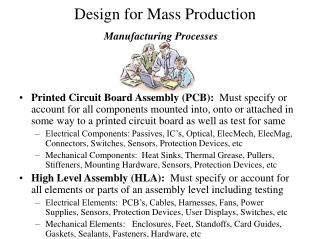
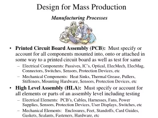
Printed Circuit Boards; PCB • Packaged integrated circuits are combined with other ICs as building blocks for a larger system. • Printed circuit board (PCB) is the substrate for the final interconnections.