Download
1 / 41
450 likes | 627 Views
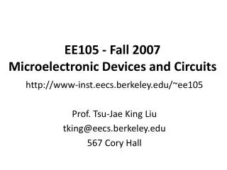
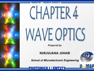
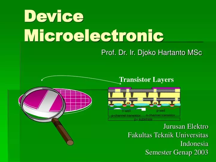
Transistor Layers. p-well. n-well. n-channel transistor. p-channel transistor. p+ substrate. Device Microelectronic. Prof. Dr. Ir. Djoko Hartanto MSc. Jurusan Elektro Fakultas Teknik Universitas Indonesia Semester Genap 2003. SAP. Satuan Acara Pengajaran. SKS : 3 Staf Pengajar

E N D
Transistor Layers p-well n-well n-channel transistor p-channel transistor p+ substrate Device Microelectronic Prof. Dr. Ir. Djoko Hartanto MSc Jurusan Elektro Fakultas Teknik Universitas Indonesia Semester Genap 2003
SAP Satuan Acara Pengajaran • SKS : 3 • Staf Pengajar • PJ: Prof. Dr. Ir. Djoko Hartanto MSc. (DH) • Ang: Arief Udhiarto, ST. (AU) • Sistem Kelas : Tunggal • Sistem Evaluasi (dalam %) • (20) Tugas. • (30) Midtest, • (30) UAS, • (20) Seminar
Pre-Test • Sebutkan empat tahap utama dalam proses microchip fabrication ! • Apa yang dimaksud dengan photolithography? • Apa fungsi packaging dalam proses pabrikasi?
silicon substrate monocrystalline polycrystalline epitaxial silicon growth polysilicon silicon dioxide oxide silicon nitride metal dopant doping concentration diffusion field effect transistor source, drain, gate Terms and Concepts to be Covered in this Lesson
MOS NMOS technology n-channel PMOS technology p-channel CMOS technology p-well n-well photoresist photomask exposure diffusion thin films photolithography etch ion implant polish, CMP planarization strips and cleans test and sort Terms and Concepts to be Covered in this Lesson
Concentration P-type N-type lightly doped p- n- very lightly doped p-- n-- heavily doped p+ n+ very heavily doped p++ n++ Variations in Dopant Concentrations
Processing Overview Processing Overview Tahap-tahap pabrikasi chip IC • Material Preparation Convert silicon dioxside to semiconductor-grade silicon • Crystal Growth and Wafer Preparation Convert polysilicon to silicon wafer • Crystal growing • Slice cutting and polishing • Photomask manufacturing
Procesing Overview Processing Overview • Wafer Fabrication • Cleaning of surfaces • Growth of epitaxial layer • Thermal oxidation of silicon • Patterning of the various layers (lithography) • Diffusion of impurities into silicon • Ion implantation of impurities
Wafer Fabrication Processing Overview • Chemical vapor deposition of polycristalline silicon • Etching of silicon and GaAs • Deposition of insulating layers (silicon oxide or nitride) • Etching of insulating layers (silicon oxide or nitride) • Depositon of conductive layers (metal, polysilicon, other) • Alloying (sintering) to form metal-silicon electrical contact
Wafer Fabrication Processing Overview • Backgrinding (thinning of wafer by grinding) • Multiprobing (DC electrical testing of each IC on wafer)
4. Packaging Processing Overview • Cutting or breaking of wafers into individual chips • Packaging of individual chips • Full AC dan DC electrical testing of packaged ICs
metal connection to gate polysilicon gate doped silicon top nitride metal connection to drain metal connection to source field oxide gate oxide oxide drain source silicon substrate gate oxide Fabrication process of a simple metal oxide semiconductor (MOS) transistor
silicon substrate The manufacture of a single MOS transistor begins with a silicon substrate.
field oxide oxide silicon substrate A layer of silicon dioxide (field oxide) provides isolation between devices manufactured on the same substrate.
Photoresist provides the means for transferring the image of a mask onto the top surface of the wafer. photoresist oxide silicon substrate
Ultraviolet light exposes photoresist through windows in a photomask. Ultraviolet Light Chrome plated glass mask Shadow on photoresist Exposed area of photoresist photoresist oxide silicon substrate
Ultraviolet light exposes photoresist through windows in a photomask. Ultraviolet Light Chrome plated glass mask Shadow on photoresist Exposed area of photoresist photoresist oxide silicon substrate
Exposed area of photoresist Unexposed area of photoresist photoresist oxide silicon substrate Exposed photoresist becomes soluble and can be easily removed by the develop chemical.
photoresist photoresist oxide silicon substrate Unexposed photoresist remains on surface of oxide to serve as a temporary protective mask for areas of the oxide that are not to be etched. Shadow on photoresist
photoresist oxide oxide silicon substrate silicon substrate Areas of oxide protected by photoresist remain on the silicon substrate while exposed oxide is removed by the etching process.
field oxide oxide oxide silicon substrate silicon substrate The photoresist is stripped off -- revealing the pattern of the field oxide.
thin oxide layer gate oxide oxide oxide silicon substrate A thin layer of oxide is grown on the silicon and will later serve as the gate oxide insulator for the transistor being constructed.
gate oxide oxide oxide silicon substrate The gate insulator area is defined by patterning the gate oxide with a masking and etching process.
gate oxide gate oxide polysilicon oxide oxide silicon substrate Polysilicon is deposited and will serve as the building material for the gate of the transistor.
ultra-thin gate oxide polysilicon gate gate gate oxide oxide silicon substrate The shape of the gate is defined by a masking and etching step.
ion beam Scanning direction of ion beam implanted ions in active region of transistors photoresist Implanted ions in photoresist to be removed during resist strip. gate gate oxide oxide drain source silicon substrate Dopant ions are selectively implanted through windows in the photoresist mask.
doped silicon gate gate oxide oxide drain source silicon substrate The source and drain regions of the transistor are made conductive by implanting dopant atoms into selected areas of the substrate.
top nitride gate drain source silicon substrate A layer of silicon nitride is deposited on top of the completed transistor to protect it from the environment.
contact holes gate drain source silicon substrate Holes are etched into selected parts of the top nitride where metal contacts will be formed.
metal contacts gate oxide oxide drain source silicon substrate Metal is deposited and selectively etched to provide electrical contacts to the three active parts of the transistor.
metal connection to gate polysilicon gate doped silicon top nitride metal connection to drain metal connection to source field oxide gate oxide oxide drain source silicon substrate gate oxide Completed structure of a simple MOS transistor
Thin Films Polish Etch Photo Diffusion Implant Test/Sort Manufacturing Areas in Wafer Fab Wafer Fabrication (front-end) Bare silicon wafer Completed product
Common Terms in Wafer Fab • Diffusion • high temperature processes • atmospheric - low vacuum pressures • oxidation, anneal, alloy, deposition, diffusion • Photolithography • patterning process (masking) • photoresist coating • exposure to UV light • develop
Common Terms in Wafer Fab • Etch • selective removal of specific materials • permanent patterning of wafer • low vacuum - high vacuum pressure • RF power, plasma etching • Ion Implant • selective doping of specific areas of wafer • through windows in photoresist or oxide • high voltage, high vacuum, ion acceleration
Common Terms in Wafer Fab • Thin Films • moderate temperatures • low vacuum - high vacuum pressures • dielectric films, metals, anneal • Polish • chemical mechanical polish (CMP) • planarization of wafer surface
Common Terms in Wafer Fab • Strips & Cleans • dry, plasma resist strip • wet, chemical cleans using acid solutions and solvents • Test/Sort • automated testing of each die on wafer • discriminate good from bad • determines a fab’s yield • ship to assembly & packaging
Thin Films Polish Etch Photo Diffusion Test/Sort Implant Typical Wafer Flow in CMOS Fab
CMOSInverter Technology VSS VDD Vin g g s s d d Vout VDD VSS Vin s g d s d g Vout n-channel transistor p-channel transistor polysilicon gate contact metal field oxide n+ p+ n+ p+ source drain source drain p-well n-substrate gate oxide Schematic Diagram Top view of Transistor Cross-section of Transistor