Download

1 / 26
260 likes | 471 Views
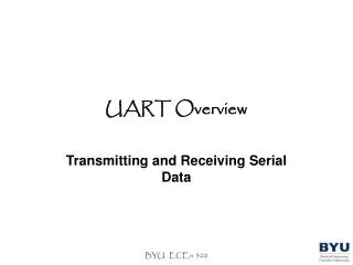
Project Check-off 2 UART Design. Jeffrey Tsai. Project Thus Far. Main Control FSM. Collision. SRAM. Packet Logic. UART IN. FIFO. UART OUT. FIFO. Audio Out interface. Audio In interface. UART. Message Definition Super-sampling Receiver Implementation Transmitter Implementation

E N D
Project Check-off 2UART Design Jeffrey Tsai
Project Thus Far Main Control FSM Collision SRAM Packet Logic UART IN FIFO UART OUT FIFO Audio Out interface Audio In interface
UART • Message Definition • Super-sampling • Receiver Implementation • Transmitter Implementation • Xilinx and Debugging tips (time permitting)
TX Idle Start D0 D1 D2 D3 D4 D5 D6 D7 Stop Idle Time TX_E Figure 3: A UART transmission. Message Definition • A low start bit followed by 8 data bits and a high stop bit. (clock is 250kHz) • The wire is normally high.
Sample Here Serial data input Super-Sampling • We watch the incoming wire at 8 times the send rate. (2MHz) • This makes it so we can catch a 250Khz message even if its phase is different from our internal 250KHz clock.
UART SERIAL-IN.H D[7:0] OE.L DRDY.H RESET.H Clock Receiver Implementation • Nick Weaver’s UART – Receive design. • Inputs: Serial-In, Reset, Clock • Outputs: D[7:0], DRDY (data-ready)
How do I start?!? • If the incoming message is 10 bits in length, and we super-sample at 8x, the message is complete when we receive 80 bits of data. • How do we keep track of where I am in the message?
8-bit Binary Counter • 3 Inputs to figure out : R, CE, C • CE is on as long as you are receiving a new message • C is the super-sampled clock frequency, NOT the incoming baud rate • R is used to reset the counter once the message is complete
Count Enable • Should be high when the input initially drops low for the start bit. • Should stay high for the duration of the message by means of a PROCEED signal. • CE = INPUT’ + PROCEED
Clock • You’ve seen how to divide clocks already from previous labs. • The clock that’s available on the board already (not from the Xchecker) is 16MHz. • Use a binary counter to divide it. • Sticky point: You send at 250kHz, you sample at 2MHz, your circuit needs one faster than that. Probably 8MHz.
Reset • Should be reset when the counter enable is low. • When the RESET button on the board is pressed, the counter should reset. • When the message is done, and DRDY goes high (data ready), this should be reset for safety/reliability reasons. • R = CE’ + RESET + DRDY
PROCEED • Intuitively, it should catch the first super-sampled bit, and stay high for the duration of the message. • This should be done with a flip-flop. • PROCEED = INPUT’ + PROCEED • But we sample from the middle of each signal, so instead, we use Q2 (3rd bit from right of the counter)
There’s more! • But this feedback loop will loop high forever! • So when DRDY or RESET is asserted, PROCEED must be forced low. • PROCEED = DRDY’ RESET’ (Q2+PROCEED)
Shift Register • Inputs the data serially and outputs it to the rest of our design in a parallel fashion. • All we need to determine is CE for the shift register. • Since we sample on the forth super-sample per sample, just look at counter. • CE = Q0’ Q1’ Q2
Why just the last 3 bits? • 4 = 00000100 • 12 = 00001100 • 20 = 00010100 • 28 = 00011100 • 36 = 00100100 • Etc.
When do we stop? • This design uses a 8-bit shift register to save space. Thus, we don’t want the stop bit to be shifted in. • We want to stop at 9*8+3 = 75 • 75= 01001011 • DRDY = Q6 Q3 Q2’ Q1 Q0 • UART-RECEIVE IS DONE!
UART-RECEIVE SUMMARY • 8 Bit counter:CE = INPUT’ + PROCEED R = CE’ + RESET + DRDY C = 2MHz Clk • Proceed: PROCEED = DRDY’ RESET’ (Q2+PROCEED) • Shift Register:CE = Q0’ Q1’ Q2 DRDY = Q6 Q3 Q2’ Q1 Q0
UART-RECEIVE (cont) • Do not take this for granted! • I defined the important signals, the rest are trivial. • Make sure you UNDERSTAND the design rather than just plugging it in!
Transmitting UART / TX SERIAL-OUT.H (TX) D[7:0] SEND.H OUTPUT_ENABLE (TX_E) RESET.H Clock Figure 2: UART Transmitter symbol. What about transmit? • Well, you tell me.
Specs for UART-Transmit • The signal you send must comply with our message definition. • A interrupt input (reset) is needed so back-off is possible. (remember that in the project, if what you read back isn’t what you wrote, you must stop transmitting) • Need TX_E to be high while transmitting and low otherwise.
General Tips • KISS (keep it simple stupid) If you have no clue what your circuit does, chances are, neither does anyone else. • Don’t be afraid to play around with the signals in a way that makes it easy for you to debug. • Learn to use the oscilloscope!
Playing with bus wires • A complicated bus lets you combine multiple wires together to form a bus. • Remember that a bus is just a collection of wires! • Useful if you a bunch of signals that aren’t named to same into a bus.
Bus wires (cont.) • Notice the Simple Box on top right is unchecked (its checked by default) • Now I can specify each signal individually. Separate each one by comma.
That’s All! • Good luck and start early!