Download
1 / 15
160 likes | 201 Views
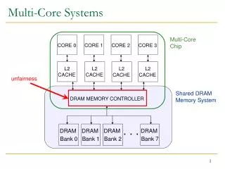
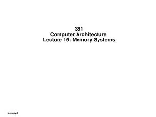
Lecture 15: DRAM Main Memory Systems. Today: DRAM basics and innovations (Section 2.3). Memory Architecture. Processor. Bank. Row Buffer. Memory Controller. Address/Cmd. DIMM. Data. DIMM: a PCB with DRAM chips on the back and front

E N D
Lecture 15: DRAM Main Memory Systems • Today: DRAM basics and innovations (Section 2.3)
Memory Architecture Processor Bank Row Buffer Memory Controller Address/Cmd DIMM Data • DIMM: a PCB with DRAM chips on the back and front • Rank: a collection of DRAM chips that work together to respond to a • request and keep the data bus full • A 64-bit data bus will need 8 x8 DRAM chips or 4 x16 DRAM chips or.. • Bank: a subset of a rank that is busy during one request • Row buffer: the last row (say, 8 KB) read from a bank, acts like a cache
DRAM Array Access 16Mb DRAM array = 4096 x 4096 array of bits 12 row address bits arrive first Row Access Strobe (RAS) 4096 bits are read out Some bits returned to CPU 12 column address bits arrive next Column decoder Column Access Strobe (CAS) Row Buffer
Organizing a Rank • DIMM, rank, bank, array form a hierarchy in the • storage organization • Because of electrical constraints, only a few DIMMs can • be attached to a bus • One DIMM can have 1-4 ranks • For energy efficiency, use wide-output DRAM chips – better • to activate only 4 x16 chips per request than 16 x4 chips • For high capacity, use narrow-output DRAM chips – since the • ranks on a channel are limited, capacity per rank is boosted • by having 16 x4 2Gb chips than 4 x16 2Gb chips
Organizing Banks and Arrays • A rank is split into many banks (4-16) to boost parallelism • within a rank • Ranks and banks offer memory-level parallelism • A bank is made up of multiple arrays (subarrays, tiles, mats) • To maximize density, arrays within a bank are made large • rows are wide row buffers are wide (8KB read for a • 64B request, called overfetch) • Each array provides a single bit to the output pin in a • cycle (for high density)
Row Buffers • Each bank has a single row buffer • Row buffers act as a cache within DRAM • Row buffer hit: ~20 ns access time (must only move • data from row buffer to pins) • Empty row buffer access: ~40 ns (must first read • arrays, then move data from row buffer to pins) • Row buffer conflict: ~60 ns (must first precharge the • bitlines, then read new row, then move data to pins) • In addition, must wait in the queue (tens of nano-seconds) • and incur address/cmd/data transfer delays (~10 ns)
Reads and Writes • A single bus is used for reads and writes • The bus direction must be reversed when switching between • reads and writes; this takes time and leads to bus idling • Hence, writes are performed in bursts; a write buffer stores • pending writes until a high water mark is reached • Writes are drained until a low water mark is reached
Open/Closed Page Policies • If an access stream has locality, a row buffer is kept open • Row buffer hits are cheap (open-page policy) • Row buffer miss is a bank conflict and expensive • because precharge is on the critical path • If an access stream has little locality, bitlines are precharged • immediately after access (close-page policy) • Nearly every access is a row buffer miss • The precharge is usually not on the critical path • Modern memory controller policies lie somewhere between • these two extremes (usually proprietary)
Address Mapping Policies • Consecutive cache lines can be placed in the same row • to boost row buffer hit rates • Consecutive cache lines can be placed in different ranks • to boost parallelism • Example address mapping policies: • row:rank:bank:channel:column:blkoffset • row:column:rank:bank:channel:blkoffset
Scheduling Policies • FCFS: Issue the first read or write in the queue that is • ready for issue • First Ready - FCFS: First issue row buffer hits if you can • Stall Time Fair: First issue row buffer hits, unless other • threads are being neglected
Refresh • Every DRAM cell must be refreshed within a 64 ms window • A row read/write automatically refreshes the row • Every refresh command performs refresh on a number of • rows, the memory system is unavailable during that time • A refresh command is issued by the memory controller • once every 7.8us on average
Error Correction • For every 64-bit word, can add an 8-bit code that can • detect two errors and correct one error; referred to as • SECDED – single error correct double error detect • A rank is now made up of 9 x8 chips, instead of 8 x8 chips • Stronger forms of error protection exist: a system is • chipkill correct if it can handle an entire DRAM chip • failure
Modern Memory System .. .. .. .. .. .. PROC • 4 DDR3 channels • 64-bit data channels • 800 MHz channels • 1-2 DIMMs/channel • 1-4 ranks/channel .. ..
Cutting-Edge Systems .. .. SMB PROC .. .. • The link into the processor is narrow and high frequency • The Scalable Memory Buffer chip is a “router” that connects • to multiple DDR3 channels (wide and slow) • Boosts processor pin bandwidth and memory capacity • More expensive, high power
Title • Bullet