Download

1 / 37
400 likes | 827 Views
ECE 2211 Microprocessor and Interfacing Chapter 8 The 8088/8086 Microprocessors and their memory and I/O interfaces. Br. Athaur Rahman Bin Najeeb Room 2.105 Email: athaur@iium.edu.my Website: http://eng.iiu.edu.my/~athaur Consultation : Tuesday 10.00 am ( appointment).

E N D
ECE 2211 Microprocessor and InterfacingChapter 8The 8088/8086 Microprocessors and their memory and I/O interfaces Br. Athaur Rahman Bin Najeeb Room 2.105 Email: athaur@iium.edu.my Website: http://eng.iiu.edu.my/~athaur Consultation : Tuesday 10.00 am ( appointment)
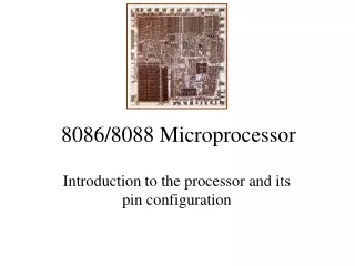
8086 Minimum-Mode Signals Power supply Vcc GND INTR _____ INTA _____ TEST NMI RESET HOLD HLDA Address / data bus AD0-AD15, A16/S3-A19/S6 ALE ____ BHE/S7 M/IO’ DT/R’ ___ RD ___ WR ____ DEN READY Interrupt interface 8086 MPU Memory/IO controls DMA interface Mode Select MN/MX’ CLK
SYSTEMCLOCK Clock (CLK) : input signal which synchronize the internal and external operations of the microprocessor.
CLOCKGENERATOR IC • The clock source is generated by 8284 ( clock generator and Driver IC ) • CLK ( 8) of 8284 is connected to pin 19 8088/8086 • 8284 also supplies it with 2 of it's control lines – RESET and READY. The RESET signal does resets the 8088. This line can also be used by other peripherals on the computer so that they reset when the 8088 resets. • READY used to slow down the 8088 ; Dfrom IO circuit thru RD1 and RD2 • A crystal oscillatoris connected between X1 and X2 which provides a FUNDAMENTAL CRYSTAL FREQUENCY. ( FCF) • 33% duty cycle the FCF is divided by 3 internally by 8244 to provide the necessary CLK • output pin pclk provide 50% of duty cycle to drive periperal devices http://en.wikipedia.org/wiki/Crystal_oscillator
BUS CYCLE AND TIME STATES • A bus cycle defines the basic operation that a microprocessor performs to communicate with external devices. • Examples of bus cycle are memory read, memory write, input/output read and input/output write. • A bus cycle corresponds to a sequence of events that starts with an address being output on the system bus followed by a read or write data transfer. • During these operations, a series of control signal are also produced by the MPU to control the direction and timing of the bus. • Each bus cycle consists of at least four clock periods, T1, T2, T3 and T4. • These clock period are also called T-state. • These 4 clock states gives a bus cycle duration of ( 125 ns * 4 ) = 500 ns in a 8-Mhz 8088 • Idle State: no bus activity ; one clock period • Wait state : controlled by READY signal ; inserted between T3 and T4 when READY = 0 . Bus cycle will complete when READY = 1
Timer States • • T1 • – Address placed on bus • – ALE active • • T2 • – Change direction of Data bus for READ instructions • • T3-4 • – Data transfer occurs
Bus Cycle and Time States T1- start of bus cycle. Actions include setting control signals to give the required values for ALE, DTR, IO/M putting a valid address onto the address bus. T2 - the RD or WR control signals are issued, DEN is asserted and in the case of a write, data is put onto the data bus. The DEN turns on the data bus buffers to connect the CPU to the external data bus. The READY input to the CPU is sampled at the end of T2 and if READY is low, a wait state TW (one or more) is inserted before T3 begins. T3 - this clock period is provided to allow memory to access the data. If the bus cycle is a read cycle, the data bus is sampled at the end of T3. T4 - all bus signals are deactivated in preparation for the next clock cycle. The 8088 also finishes sampling the data (in a read cycle) in this period. For the write cycle, the trailing edge of the WR signal transfers data to the memory or I/O, which activates and write when WR returns to logic 1 level.
System Timing Diagrams T-State: • One clock period is referred to as a T-State T-State • An operation takes an integer number of T-States CPU Bus Cycle: • A bus cycle consists of 4 or more T-States T1 T2 T3 T4
Wait and Idle States • Idle State – No bus activity required – Each is 1 clock period long – Occurs when instruction queue is full or the MPU does not need to read/write to memory • Wait State – Triggered by events external to MPU – Buffer full will trigger a wait state – Triggered by READY pin – Inserted between T3 and T4
What is the duration of the bus cycle in the 8088 based microcomputer if the clock is 8MHz and two wait states are inserted The duration of the bus cycle is in an 8MHz system is given in general by Tcyc = 500 ns + N x 125ns Tcyc = 500 ns +2 x 125ns = 750 ns
What is the duration of the bus cycle in the 8086 based microcomputer if the clock is 5MHz a)No wait state ? b)with three wait states are inserted.
Hardware Organization of the memory Address Space Low / Even Bank High / Odd Bank 8086 8088 Bank – select signals
Byte / Word Transfer 8088 8088 byte transfer 8088 word transfer
Question A memory cycle for an 8088 running at 5Mhz has no wait / idle state. What is the duration for A) to write a byte into memory B) to write a word into memory
Y X + 1 X Y + 1 ____ BHE ( HIGH ) Address bus A19 – A1 D15 – D8 D7 – D0 A0(LOW) 8086 byte access on even address ( low) A0 is set to 0 to enable low bank BHE is set to logic 1 to disable high bank Data is transferred via D0 ( LSB ) – D7 ( MSB )
Y X + 1 X Y + 1 ____ BHE ( LOW ) Address bus A19 – A1 D15 – D8 D7 – D0 A0(HIGH) 8086 byte access on odd address ( high bank) A0 is set to 1 to disable low bank BHE is set to logic 0 to enable high bank Data is transferred via D8 ( LSB ) – D15 ( MSB )
Y + 1 Y X + 1 X ____ BHE ( LOW ) Address bus A19 – A1 D15 – D8 D7 – D0 8086 word access on even address ( lowbank) - aligned Both A0 and BHE is enabled ; data transferred from both banks at same time Data is transferred via D0 ( LSB ) – D15 ( MSB ) Aligned and occurs in 1 bus cycle
8086 word access on odd address ( high bank) A word starting at ODD address : Misaligned The LSB is located at lower address in High Bank,( Example : 00003(h) and 00004(h) Requires 2 bus cycles, where X+1 address in high bank is accessed during the first Bus cycle ( A0=1, BHE=0) and data is transferred using D8 to D15 In second bus cycle ( A0 = 0, BHE = 1 , data transferred via D0 – D7 ) The next two slaids demonstrated this activity
X + 3 ODD ADDRESS WORD TRANSFER BY THE 8086 X + 2 X + 1 X A0(HIGH) ____ BHE ( LOW ) Address bus A19 – A1 D15 – D8 D7 – D0 First bus cycle
X + 3 ODD ADDRESS WORD TRANSFER BY THE 8086 X + 2 X + 1 X A0(LOW) ____ BHE ( HIGH ) Address bus A19 – A1 D15 – D8 D7 – D0 Second bus cycle