Download

1 / 22
220 likes | 374 Views
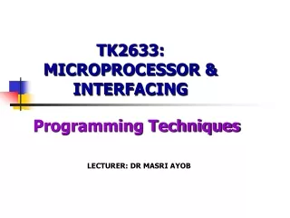
ECE 371 Microprocessor Interfacing. Unit 1b - Introduction to the MC9S12DP256B Microcontroller. 16-bit Microcontroller Family (Partial List). • MC9S12D64 MC9S12DG128B MC9S12DP256B (our chip) MC9S12DP512. Product Numbering System. MC 9 S12 DP 256 B Status. Memory type. - 9:flash.

E N D
ECE 371Microprocessor Interfacing Unit 1b - Introduction to the MC9S12DP256B Microcontroller
16-bit Microcontroller Family (Partial List) • MC9S12D64 • MC9S12DG128B • MC9S12DP256B (our chip) • MC9S12DP512
Product Numbering System MC 9 S12 DP 256 B Status Memory type - 9:flash Core type Family Approximate memory size Flash revision
68HC12 References • http://www.freescale.com • products -> microcontrollers -> 16 bit microcontrollers • documentation -> microcontrollers -> 16 bit microcontrollers • Lab Computers – Files
INTERNAL FEATURES OF MCS912DP256B (PARTIAL LIST) MEMORY A/D CONVERTER I/O PORTS PULSE-WIDTH MODULATON OUTPUTS SERIAL I/O WATCH DOG TIMER TIMER CONTROLLER AREA NETWORK (CAN) SIGNALS PULSEACCUMULATOR
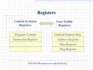
INTERNAL MEMORY OF MCS912DP256B • 12 K BYTES OF RAM (PROGRAM CODE, VARIABLES, AND STACK) • 4K BYTES OF EEPROM (SYSTEM DATA) • 256K BYTES OF FLASH EEPROM (PROGRAM CODE) • ALSO 2K BYTES FOR REGISTERS
Registers Programmable Memory Manager Internal SRAM CPU Internal EEPROM 16-bit Address 64K Internal Flash External SRAM 256K
CONNECTIONS TO THE OUTSIDE WORLD 112 PINS ON MC9S12DP256B CHIP PORTS A - 8 BITS B - 8 BITS E - 8 BITS H - 8 BITS J - 4 BITS K - 7 BITS M - 8 BITS P - 8 BITS S - 8 BITS T - 8 BITS AD0 - 8 BITS AD1 - 8 BITS TOTAL: 91 I/O BITS 13 PINS FOR INPUT VOLTAGES AND GROUND 6 PINS FOR CLOCK INPUTS AND RESET 2 OTHER PINS (BKGD, TEST) NOTE: MOST PINS HAVE MULTIPLE FUNTIONS
ALTERNATE FUNCTIONS OF PORT PINS PORTS A AND B - EXTERNAL ADDRESS/DATA BUS PORT E - 8 BITS - CONTROL SIGNALS, MODE SELECTION, INTERRUPT REQUESTS, PORT T - 8 BITS - TIMER PINS PORT S - 8 BITS - ASYNCHRONOUS SERIAL I/O (SCI) PINS PORT H - 8 BITS - SYNCHRONOUS SERIAL I/O (SPI) PINS; INTERRUPT REQUESTS PORT M - 8 BITS SPECIAL SERIAL I/O (BDLC, CAN) PORT J - 4 BITS - INTERRUPT REQUESTS; CAN SIGNALS
MORE ALTERNATE FUNCTIONS OF PORT PINS PORT P - 8 BITS - PULSE WIDTH MODULATION (PWM) OUTPUTS; INTERRUPT REQUESTS PORT K - 7 BITS - ADDRESS LINES A19-A14 FOR EXPANDED (EXTERNAL ACCESS MODE) PORT AD0 - 8 BITS - INPUTS TO A/D CONVERTER 0 PORT AD1 - 8 BITS - INPUTS TO A/D CONVERTER 1
Operating Modes • No External Addresses • No External Data Buses • Single Chip Stand Alone Mode • Port A – General Purpose I/O • Port B – General Purpose I/O • Selected by: - BKGD =1, MODB = 0, MODA = 0 • Operating Modes are Sensed at Reset Normal Single-Chip Mode
Operating Modes Normal Expanded Wide Mode • Multiplexed 16-bit Address/16-bit Data Bus • Port A – High Address and Data Bits • Port B – Low Address and Data Bits • ADDR[7:0] and DATA[7:0] • Control Signals: R/W (from PE2) ECLK (from PE4) • Selected by: - BKGD =1, MODB = 1, MODA = 1
MULTIPLEXED WIDE BUS ADDR7 - ADDR0/ DATA7 - DATA0 PB7 - PB0 ADDR 15 - ADDR8/ DATA15 - DATA8 PA7 - PA0 PE2 R/W (EXTERNAL BUS CLOCK) PE4 ECLK LSTRB PE3
Operating Modes Normal Expanded Narrow Mode • Multiplexed 16-bit Address/8-bit Data Bus • Port A – High Address and All 8 Data Bits- ADDR[15:8] and DATA[7:0] • Port B – Low Address • ADDR[7:0] • Control Signals: R/W (from PE2) ECLK (from PE4) • Selected by: - BKGD =1, MODB = 0, MODA = 1
MULTIPLEXED NARROW BUS ADDR7 - ADDR0 PB7 - PB0 PA7 - PA0 ADDR 15 - ADDR8/ DATA7 - DATA0 PE2 R/W PE4 ECLK
Access Type vs. Bus Control Pins Table 12-5 Access Type vs. Bus Control Pins /LSTRB A0 R/W Type of Access 1 0 1 8-bit read of an even address 0 1 1 8-bit read of an odd address 1 0 0 8-bit write of an even address 0 1 0 8-bit write of an odd address 0 0 1 16-bit read of an even address 1 1 1 XXX 0 0 0 16-bit write to an even address 1 1 0 XXX