Download
1 / 17
210 likes | 707 Views
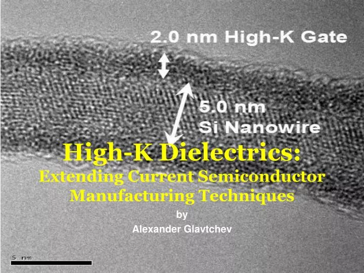
High-K Dielectrics: Extending Current Semiconductor Manufacturing Techniques. by Alexander Glavtchev. Introduction. Since the 1960’s semiconductor industry has used poly-Silicon gate with a Silicon dioxide gate dielectric layer.

E N D
High-K Dielectrics:Extending Current Semiconductor Manufacturing Techniques by Alexander Glavtchev
Introduction • Since the 1960’s semiconductor industry has used poly-Silicon gate with a Silicon dioxide gate dielectric layer. • Continuing miniaturization has thinned the SiO2 gate dielectric layerto ~5 atomic layers, or less than 2nm in thickness. • Electron tunneling is a major concern at this level as it contributes to current leakage through the gate. • Further scaling would increase the already-problematic gate current leakage (IG) and lead to power loss, increased power consumption, and generate excess heat. • New materials with high dielectric constant, k, are needed to avoid abrupt and costly technological and manufacturing process changes, reduce leakage, and improve performance.
Introduction Introduction
Physics • Research by Intel has shown that a thicker high-k dielectric gate increases overall capacitance while decreasing the leakage current by ~100X. • Transistors are becoming horizontally smaller, therefore a vertically-thicker dielectric gate is not a problem.
Why is Capacitance Important? The drive current ID for a MOSFET can be approximated by the following equation: W is the transistor channel width L is the transistor channel length μ is carrier mobility (which can be treated as a constant in this approximation) C is the capacitance density associated with the gate dielectric VG is the applied gate voltage VD is the applied drain voltage VT is the threshold voltage
Why is Capacitance Important? It can be seen that ID increases almost linearly with VD until a maximum ID is reached when: and IDS is the saturated drain current, and it results when VG≥ VT and a carrier channel has been established under the gate. Thus, it can be seen that decreasing the channel length or increasing the Capacitance will increase the drain current IDS and establish a channel beneath the gate (ON state).
Physics The capacitance of the gate can be modeled as a parallel-plate capacitor (ignoring quantum effects and depletion): where A is the Area of the capacitor and t is the thickness. Since the t is greater for the new dielectric gate material, it requires an even larger dielectric constant k to increase the overall capacitance – that’s where the new high-k dielectric materials come into play. These materials are Hafnium-based and will have k > 3.9, the dielectric constant of SiO2.
Why high-k dielectric? • Experimental data shows that a higher k has a greater effect on total capacitance than a decreasing thickness. • Furthermore, a thicker Hafnium-based dielectric gate with a metal gate increases resistance and reduces the unwanted gate leakage current.
Why high-k dielectric? • In addition, Intel has shown that the gate delay between ION/IOFF is less when using a high-k/metal gate setup instead of the traditional poly-Silicon/SiO2 setup. • This allows for faster signal transmission and a better ION/IOFF ratio, allowing for more accurate reading of the ones and zeros of binary data.
Challenges and Issues • The poly-Si gate is not electromagnetically compatible with the new high-k dielectric. • Phonon scattering and Fermi level pinning. • New manufacturing methods for atomic level deposition needed. • Short-term solution - additional advances in lithography and technology are needed to improve performance in the long run.
Metal Gate vs. SiO2 • Phonon scattering is greater using a high-k/poly-Si dielectric than the traditional SiO2/poly-Si. • This leads to decreased channel mobility. • Use of a metal gate can help increase the surface mobility.
The Future • High-k dielectrics are vital for next-generation low power-consumption, low leakage, high performance logic devices. • Non-silicon high-mobility materials may require extensive use of high-k dielectrics (e.g. Ge, III-V quantum wells, carbon nanotubes). • Formation and compatibility of high-k dielectrics better with non-silicon materials (non SiO2-based).
The Future • Use of non-silicon Ge substrate with a high-k and a metal gate increases the total capacitance. High-k dielectrics are more compatible with non-Si materials. • Intel has shown that formation of high-k dielectric on Ge is of greater quality than forming SiO2 on Ge.
Sources • www.intel.com • www.wikipedia.com • www.computer.org • High-k gate dielectrics: Current status and materials properties considerations. Journal of Applied Physics, Vol. 89, No. 10.