Download
1 / 68
680 likes | 1.1k Views
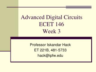
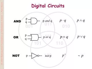
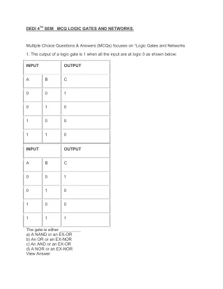
Chapter 3 Digital Circuits. The knowledge of the electrical aspects of digital circuits ( 数字电路中的电气知识). A Z 0 1 1 0. A B Z. A B Z. 0 0 0 0 1 0 1 0 0 1 1 1. 0 0 0 0 1 1 1 0 1 1 1 1. A. Z. B. A. Z. A. &. Z. B.

E N D
Chapter 3 Digital Circuits The knowledge of the electrical aspects of digital circuits (数字电路中的电气知识)
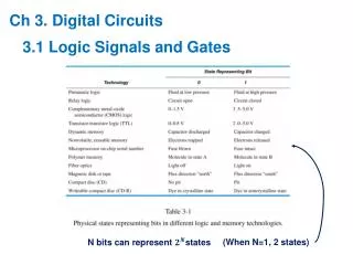
A Z 0 1 1 0 A B Z A B Z 0 0 0 0 1 0 1 0 0 1 1 1 0 0 0 0 1 1 1 0 1 1 1 1 A Z B A Z A & Z B ≥1 =1 3.1 Logic Signals and Gates (逻辑信号与门电路) • Basic logic gates OR gate AND gate NOT gate Logic expression (逻辑表达式) Z = A·B Z = A+B Z = A’ Truth table (真值表) Logic Symbol (逻辑符号)
A B Z A B Z 0 0 1 0 1 1 1 0 1 1 1 0 0 0 1 0 1 0 1 0 0 1 1 0 A Z A B Z B & ≥1 3.1 Logic Signals and Gates (逻辑信号与门电路) • Basic logic gates NOR gate(或非门) NAND gate (与非门) Logic expression (逻辑表达式) Z = ( A·B ) ’ Z = ( A+B ) ’ Truth table (真值表) Logic Symbol (逻辑符号)
0 1 positive logic 正逻辑 0 1 positive 正逻辑 negative 负逻辑 3.1 Logic Signals and Gates • How to express logic 0 and 1 in physical circuits? HIGH (高电平) Logic 1 LOW(低电平) Logic 0
Vcc R VOUT VIN 3.1 Logic Signals and Gates • How to express logic 0 and 1 in physical circuits? Asimple circuit to get High level and Lowlevel: • Switch on,Vout= 0 V (LOW) • Switch off,Vout= Vcc (HIGH) S 可以做开关的器件?
3.2 Logic Family (逻辑系列) • Logic family: A collection of different IC chips that have similar input, output, and internal circuit characteristics, but that perform different logic functions. • Ordinary logic family: TTLLogic, CMOSLogic • Attention: • Chips from the same family can be interconnected to perform any desired logic function. • Chips from differing families may not be compatible.
5.0V Logic 1(HIGH) Logic 0(LOW) 3.5V 1.5V 0.0V 3.3 CMOS Logic 1. CMOS logic levels Typical:5V power supply undefined Other power supply:3.3V or 2.7V
源极 source 漏极 drain N channel Vgs 栅极 gate + 栅极 gate + Vgs 漏极 drain 源极 source P channel 3.3 CMOS Logic N-channel and P-channel 2. MOS Transistors • ( Normally, Vgs≥0 ) • for Vgs=0, • Rds is very high(>106) • 截止状态(off) • Vgs →Rds • 过渡到导通状态(on)
源极 source Vgs + 栅极 gate 漏极 drain P channel 3.3 CMOS Logic N-channel and P-channel 2. MOS Transistors • ( Normally:Vgs≤0 ) • for Vgs = 0, • Rds is very high • 截止状态(off) • Vgs→Rds • 过渡到导通状态(on)
3.3 CMOS Logic N-channel and P-channel 2. MOS Transistors • Attention: • MOS晶体管栅极阻抗非常高(>1兆欧). • 无论栅电压如何,栅-源、栅-漏之间几乎没有电流(漏电流 leakage current : <1A). • 栅-源、栅-漏之间有电容耦合. 信号转换时,电容充放电,功耗较大。 理想状态下(不考虑电容、电阻效应),MOS 管可看作受控开关.
Vcc R Vout VDD Vin RD Vout D iD G Vin S 3.3 CMOS Logic 2. MOS Transistors • Basic Switch Circuit(基本开关电路) • 输入为低,截止状态 (off),输出为高. • 输入为高,导通状态 (on),输出为低.
VDD = +5.0V Tp S Vout Vin D Tn G S 3.3 CMOS Logic (基本CMOS反相器) 3. Basic CMOS Inverter Circuit NMOSand PMOS transistors are used together in a complementary way to form CMOS logic. Basic Principles: (1) When Vin = 0.0V (Low), Tp on, Tn off. VOUT 5.0 V (High). (2) When Vin = 5.0V (High), Tp off, Tn on. VOUT 0.0 V (Low). 没有大的工作电流流过MOS管,功耗较低.
VDD = +5.0V VDD Tp S Vout Z “低”有效 Vin D Tn G A S 3.3 CMOS Logic (基本CMOS反相器) 3. Basic CMOS Inverter Circuit NMOSand PMOS transistors are used together in a complementary way to form CMOS logic.
VDD = +5.0V T2 T4 Z A T1 B T3 3.3 CMOS Logic 4. CMOS NAND and NOR Gates • NAND 1) Both inputs are HIGH T1, T3all on; T2, T4 all off. So, Z 0.0V (Low) 2) Either input is LOW at least one of T1 and T3 is off, at least one of T2 and T4 is on. So, Z VDD (High) Z = ( A·B ) ’
VDD = +5.0V A T2 B T4 Z T1 T3 3.3 CMOS Logic 4. CMOS NAND and NOR Gates • NOR 1) Both inputs are LOW T1, T3all off; T2, T4 all on. So, Z VDD (High) 2) Either input is HIGH at least one of T1 and T3 is on, at least one of T2 and T4 is off. So, Z 0.0V (Low) Z = ( A+B ) ’
VDD = +5.0V VDD = +5.0V A Z B A Z B 3.3 CMOS Logic 4. CMOS NAND and NOR Gates 小结: • 每个输入控制一对互补的晶体管.(P接1,N接0) • 基本逻辑体现在N网络上,P网络采用对偶形式. • 输出反相(取非).
VDD = +5.0V A B Z C D 3.3 CMOS Logic 5. AND-OR-INVERT and OR-AND-INVERT Gates • AND-OR-INVERT (与或非门) CD AB Z = (A·B + C·D)’
C D A B 3.3 CMOS Logic 5. AND-OR-INVERT and OR-AND-INVERT Gates • OR-AND-INVERT (或与非门) Z =[(A+B)·(C+D)]’
3.3 CMOS Logic 6. Fan-In(扇入) • Fan-In:The number of inputs that a gate can have in a particular logic family. (门电路所具有的输入端数目.) • The additive “on” resistance of series transistors limits the fan-in of CMOS gates. (导通电阻的可加性限制了CMOS门的扇入数.) Typically,NOR gates: ≤4 NANR gates: ≤6
3.3 CMOS Logic 6. Fan-In(扇入) • Gates with a larger number of inputs can be composed by cascading gates with fewer inputs. (较多输入的门电路可由较少输入的门电路级联而构成.)
VDD = +5.0V Z A 3.3 CMOS Logic 7. Noninverting Gates(非反相门) • A logical inversion comes “for free”; • It is not possible to design a noninverting gate with a smaller number of transistors than an inverting one. Noninverting buffer (非反相缓冲器) 2-input AND gate
3.4 Electrical Behavior of CMOS Circuits(CMOS电路的电气特性) • Logic Voltage levels(逻辑电压电平) • DC noise margins(直流噪声容限) • Fanout(扇出) • Speed(速度) • Power consumption(功耗) • Noise(噪声) • Electrostatic discharge(静电放电) • Open-drain outputs(漏极开路输出) • Three-state outputs(三态输出) 物理上的 而不是逻辑上的
3.5 3.11 3.12 (功能表可以不画) Homework
VDD = +5.0V Tp 1 VOUT VOUT 1 0 5.0 VIN Tn 0 VIN 1.5 3.5 5.0 Typical transfer character 3.5 CMOS Steady-State Electrical Behavior (CMOS稳态电气特性) 1. Logic Levels and Noise Margins (逻辑电平和噪声容限)
VOHmin HIGH ABNORMAL LOW VIHmin VILmax VOLmax • Logic Levels • VOHmin: • VIHmin : • VILmax : • VOLmax : VCC-0.1V 0.7VCC 0.3VCC GND+0.1V
VOHmin HIGH ABNORMAL LOW VIHmin VILmax VOLmax • DC noise margin(直流噪声容限) A measure of how much noise it takes to corrupt a worst-case output voltage into a value that may not be recognized properly by an input. ——一种对噪声容忍程度的量度. Gate 1 Gate 2 • HIGH-state noise margin: VNH=VOHmin- VIHmin • LOW-state noise margin: VNL=VILmax- VOLmax
Example: Compute the LOW-state and HIGH-state DC noise margins. Table 3-6 (p.146) Table 3-7 (p.147) 74HC Family VOHminC = 4.4V VOLmaxC = 0.1V VIHmin = 3.85V VILmax = 1.35V 74HCT Family VOHminC= 4.4V VOLmaxC= 0.1V VIHmin = 2.0V VILmax = 0.8V • 74HC driving 74HCT • HIGH-state: 4.4 – 2.0 = 2.4V • LOW-state: 0.8 – 0.1 = 0.7V • 74HCTdriving 74HC • HIGH-state: 4.4 – 3.85 = 0.55V • LOW-state: 1.35 – 0.1 = 1.25V
VCC VCC Rp VOUT VIN Z A Rn (带电阻性负载的电路特性) 2. Circuit Behavior with Resistive Loads
VCC VCC Rp R1 Rp RThev VOUT VOUT + VThev Rn R2 Rn (带电阻性负载的电路特性) 2. Circuit Behavior with Resistive Loads
VCC = + 5.0V Rp (>1M) Vout IOLmax resistive load Rn • Sinking Current(吸收电流) If the output is LOW (VOUT≤VOLmax) Vin high,Tnon,Tp off The output is said to sink current. Sinking Current (IOLmax): The maximum current that the output can sink in the LOW state while still maintaining VOUT≤VOLmax .
VCC = + 5.0V VOHmin IOHmax Rp resistive load Rn (>1M) • Sourcing Current(提供电流) If the output is HIGH (VOUT≥VOHmin) Vin low,Tpon,Tn off The output is said to source current. Sourcing Current (IOHmax): The maximum current that the output can source in the HIGH state while stillmaintaining VOUT≥VOHmin.
VCC = + 5.0V VCC = + 5.0V RThev RThev + + VThev VThev • Estimating Sinking/SourcingCurrent • When the output is LOW, estimating sinking current: • (Rp近似断路,Rn近似短路) VOUT = 0 VIN = 1 • When the output is HIGH, estimating sourcing current:(Rp近似短路,Rn近似断路) VOUT = 1 VIN = 0
An important feature of the CMOS circuits: • The output structure by itself consumes very little current in either state, HIGH or LOW. In either state, one half of the transistors is in the high-impedance “off” state. • If there’s no load, then there’s no current flow and the power consumption is zero. • If there’s a load, current flows through both the load and the “on” transistor, and power is consumed in both.
VCC = + 5.0V VCC = + 5.0V 400 4k VOUT 4.31V VOUT 0.24V VIN 1.5V VIN 3.5V 2.5k 200 3. Circuit Behavior with Nonideal Inputs(非理想输入时的电路特性) • 非理想的输入电平,将导致晶体管的“导通” 、 “截止”状态发生改变,致使输出电平变坏。 • 更糟糕的是:输出端电流 ,功耗 。
The number of inputs that the gate can drive without exceeding its worst-case loading specifications. 在不超出其最坏情况负载规格的条件下,一个逻辑门能驱动的输入端个数。 Depending not only on the characteristics of the output, but also on the inputs that it is driving. Must be examined for both possible output states, HIGH and LOW. overall fanout = min (HIGH-state fanout, LOW-state fanout) DC fanout & AC fanout 4. fan-out( 扇出)
CMOS: 74AHC IOHmaxC = – 50 µA IOLmaxC = 50 µA IIHmax = 1 A IILmax = – 1 A CMOS: 74HC IOHmaxc = – 20 µA IOLmaxc = 20 µA IIHmax = 1 A IILmax = – 1 A Example: Compute the maximum fanout Table 3-6 (p.146) Table 3-7 (p.147) • 74AHCdriving 74HC • LOW-State fanout: • HIGH-State fanout: Overall fanout: min (HIGH-state fanout, LOW-state fanout)=50
5. Effects of Loading ( 负载效应) • Loading an output beyond its rated fanout has several effects(不良负载效应): • The output voltage gets worse. • 输出电压变差.(不符合逻辑电平的规格) • propagation delay and transition time increase. • 传输延迟和转换时间变长. • The operating temperature of the device may increase, thereby reducing the reliability and causing device failure. • 温度可能升高,可靠性降低,器件失效.
X Z +5V X Z 1k Z X 6. Unused Inputs ( 未用输入端的处理) • Unused CMOS inputs should never be left unconnected (or floating). • Method 1: Tied to a used input. Increase the capacitive load on the driving signal and may slow things down. • Method 2: An unused AND or NAND input should be tied to logic 1, • An unused OR or NOR input should be tied to logic 0.
transition time(转换时间) propagation delay(传播延迟) static power dissipation(静态功耗) dynamic power dissipation(动态功耗) 3.6 CMOS Dynamic Electrical Behavior (CMOS动态电气特性) Both the speed and the power consumption of the CMOS device depend to a large on “AC” or dynamic characteristics of the device and its load. • Speed • Power Consumption
10% 10% • Transition Time The amount of time that the output of a logic circuit takes to change from one state to another. • rise time(tr ) and fall time(tf) • Reason: • The “on” resistances of the transistors ( “导通”电阻) • stray capacitance(寄生电容)
VCC = + 5.0V Rp RL + CL VL Rn • Transition Time • 电容两端电压不能突变. 在实际电路中可用时间常数近似转换时间.
VIN VOUT • Propagation delay The amount of time that it takes for a change in the input signal to produce a change in the output signal.
VDD = +5.0V Tp VOUT VIN Tn CL • Power Consumption (功率损耗) 动态功耗的来源: • 两个管子瞬间同时导通产生的功耗 PT • 对负载电容充、放电所产生的功耗 PL • Static power dissipation (静态功耗) • The power consumption while the output is not changing. • Dynamic power dissipation (动态功耗) • The power consumption during state transitions.
VCC 的大小 输入波形的好坏 输入信号频率 负载电容 输入信号频率 (VCC ) 2 • Power Consumption (功率损耗) 动态功耗的来源: • 两个管子瞬间同时导通产生的功耗 PT • 对负载电容充、放电所产生的功耗 PL • Static power dissipation (静态功耗) • The power consumption while the output is not changing. • Dynamic power dissipation (动态功耗) • The power consumption during state transitions.
3.1 3.20 (只考虑驱动CMOS负载的情况) 3.27(a)(b) Homework
EN_L A B EN 3.7 Other CMOS Input and Output Structures (其他CMOS输入输出结构) • Transmission Gates (传输门) • When EN = 0, EN_L = 1 transistor “off ” A and B are disconnected. • When EN = 1, EN_L = 0 transistor “on ” a low-impedance connection. • 双向器件 • 传播延迟非常短
Logic symbol: VOUT VT- VT+ 5.0 VT+ input threshold VT- VIN 2.1 2.9 5.0 Transfer characteristic • Schmitt-Trigger Input(施密特触发器输入) Hysteresis(滞后): the difference between the two thresholds: VT+-VT-
Schmitt-Trigger Input(施密特触发器输入) ordinary inverter Schmitt-trigger inverter Device operation with slowly changing inputs