Download
1 / 98
990 likes | 1.12k Views
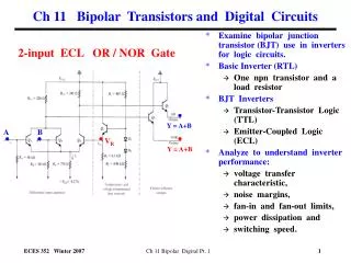
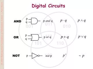
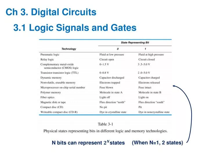
Ch 3. Digital Circuits. 3.1 Logic Signals and Gates. N bits can represent states. (When N=1, 2 states). Input. Output. Black-box. Black-box representation and Truth table shows a logic circuit with input/output and ignores electrical behavior of the circuit.

E N D
Ch3. Digital Circuits 3.1 Logic Signals and Gates • N bits can represent states • (When N=1, 2 states)
Input • Output • Black-box • Black-box representation and Truth table shows a logic circuit with input/output and ignores electrical behavior ofthe circuit
AND gate produces ‘1’ : Only if all of its inputs are ‘1’ • OR gate produces ‘1’ : One or more of its inputs are ‘1’ • NOT gate produces an output that is opposite of its input value
NAND Gate : Opposite of an AND gate’s output • NOR Gate : Opposite of an OR gate’s output
Black-box representation Truth table
Input • Lag • Lag • Lag Output • Timing diagram show how the circuit might respond • to a time-varying pattern of input signals
3.3 CMOS Logic • Not expected tooccur except during signal transition
NMOS • Turn on when • PMOS • Turn on when • High resistance : “Off” Transistor • Low resistance : “On” Transistor
PMOS, Turn on when • NMOS, Turn on when
PMOS PMOS NMOS NMOS
둘 중 하나만 On되어도 Z=‘1’ • 둘 다 On 되어야 Z=‘0’
PMOS PMOS PMOS NMOS NMOS NMOS
둘 다 On 되어야 Z=‘1’ • 둘 중 하나만 On되어도 Z=‘0’
D PMOS는 F를 이용 PMOS는 F를 이용 A B = F = D C F F NMOS는 F’를 이용 NMOS는 F’를 이용 C A = = F’ = D B • AND -> Series • OR -> Parallel
PMOS는 F를 이용 NMOS는 F’를 이용 • AND -> Series • OR -> Parallel
NAND + Inverter • More Transistors are needed than NAND
6 Transistor • 4 Transistor • 6 Transistor • 4x3+2 =14 Transistor • 16 Transistor
6 Transistor • 4 Transistor • 6 Transistor • 4x3+2 =14 Transistor • 16 Transistor
3.5 CMOS Static Electrical Behavior • Noise can be added in signals • So, There are noise margins
High state에서는 Minimum value 고려 • : Min input voltage guaranteed to be recognized as high • Low state에서는 Maximum value 고려 • : Max input voltage guaranteed to be recognized as low • : Max output voltage produced in low state • : Min output voltage produced in high state
(TTL load) • (TTL load)
Sink current • Source current
Pull-up • Pull-down
No Transition Time in ideal case • (80% ~ 20%) • (20% ~ 80%)
3.6 CMOS Dynamic Electrical Behavior • Both the speed and the power consumption of a CMOS device depend to a large extent on “AC” device
High State • Low State
Low State • High State
Ideal case (No rise and fall times) • 50% • 50% • Propagation delay
(internal power dissipation due to output transition) (Power due to load capacitor)