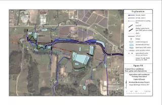
Download
1 / 33
330 likes | 443 Views
Explanation for design. The theory of computer architecture Dec 15, 2008 (Mon.). Task of Computer design theory. Design Micro Processor Reference URL: http://www.lsi-contest.com/index.html. ENJOY HDL!. That's all. About Micro Processor. behavior

E N D
Explanation for design The theory of computer architecture Dec 15, 2008 (Mon.)
Task of Computer design theory • Design Micro ProcessorReference URL:http://www.lsi-contest.com/index.html ENJOY HDL!
About Micro Processor • behavior • Fetch・・・Importing the next instruction from memory or cash. • Decode・・・With discriminating the imported instruction , defining what to do. • Execute・・・Execute the instruction. • Write Back ・・・reflecting the result. ・・・ E D C B 命令 A cycle 1 2 3 4 5 6 7 8 9 10 11 12 13 Fetch A B C D Decode A B C Execute A B C A B C Write Back
Instruction Set ~About Instructions that a microprocessor supports~
Instruction Set(1) • You make the SRP that a bubble sorting program is executable For simplicity, the usable order is set of 9 of the following (The basic task can be realized with these 9)
Instruction Set (2) add :value of register 2 + value of register 3 → store in register 1 subtract :value of register 2 - value of register 3 → store in register 1 and :Multiply value of register 2 and value of register 3 every bit →store in register 1 or :Add value of register 2 and value of register 3 every bit →store in register 1 Operation is performed only with the value of the register
Instruction Set (3) load word :value of register 2 + integer(100) = address of the memory load the value of the address → register 1 store word :value of register 2 + integer(100) = address of the memory store the value of register 1 → the address Communication is performed between register and memory
Instruction Set (4) branch on equal :value of register 1 ≠ value of register 2 → next instruction value of register 1 = value of register 2 → (1+25) instruction set on less than :value of register 2 < value of register 3 → store 1 in register 1 ≧ → 0 jump :change the address of program counter without condition Change the address of Program Counter =Change the Instruction
Addressing ~Data style~
Addressing(1) Using Byte Addressing in SRP 1 byte go up, then 1 byte address go up.
Addressing(2) Instruction size → 4 byte 4 byte address go up, then 1 word address go up. Instruction memory and date memory have 32bit address. Using Word Addressing. It is necessary to change to the Word Address for the access to the memory.
Instruction Format(1) An instruction = 32 bits To show the kind of instruction or an address of register, you divide 32 bits and use it. The divided part is called “field” and the instruction in such a bit is called “assembler expression” or “machine language expression”. decimal number is used in the table
Instruction Format(2) R-style :Show three Register Addresses I-style :Show two Register Addresses and a number J-style :There is no need to show a register address decimal number is used in the table
Instruction Format(2) R-style :Show three Register Addresses I-style :Show two Register Addresses and a number J-style :There is no need to show a register address 32767~-32768 are usable
Instruction Format(2) R-style :Show three Register Addresses I-style :Show two Register Addresses and a number J-style :There is no need to show a register address • value in table is Absolute address • unsigned /zero or positive value • The negative value is not necessary
Instruction Format(3) A name is added to each field op:operation rs :source register rt :source register (usually) rd :destination register, the place that stores a result func:function (show the variation of the op field)
Size of Instruction Memory and Data Memory 命令メモリ 0~255番地 データメモリ 256~511番地
基本動作 Read an instruction corresponding to the value of the program counter Decode an instruction and perform necessary control Read values from register fileand operate in ALU Write in an operation result anda value of the data memory at a register file ①Fetch ②Decode ③Execute ④Write back
Development environment • ISE10.1 • ModelSim • Necessary file • alu_pkg.vhdDefinition such as opecode • dram.vhdData RAM • irom.vhdInstruction ROM • SRP.vhdSRP(Here is made this time. ) • test_SRP.vhdFor test bench This project file is distributed on the Web.
SRP (Small RISC Processor ) • RISC: Reduced Instruction Set Computer • Place where code of SRP is written
② ① The value of program count is maintained Program counter’s value is selected when diverging Control of instruction ④ Execution part of operation according to instruction Instruction is load Data RAM or not ⑥ ③ ⑦ ⑧ ⑤ Select register operation or operation Instruction The address of the written register is selected by the instruction(※Instruction Set) The value of the register is rewritten, and output.
Instruction ROM&Data RAM • Instruction ROM • The instruction corresponding to input Add is output to Dout in each 10ns. • Data RAM • Read・・・Data corresponding to input Add is output to Dout in each 10ns. • Write・・・When WE is ‘1’ and Synchronize with Clock, the value of input Din is written at the address of input Add.
32ビットレジスタ About a detailed each part • It schedules it opening to the public on Web in the future. • Exampleabout ①・32 bit register・Synchronize with Clock・Reset by signal Reset nextpc 32 pc 32 Reset Clock
What is Bubble Sort !? • The 1st and the 2nd are compared. • The 2nd and the 3rd are compared. • The last number is fixed . It repeats while the part that has not been fixed. Initial data: 8 4 3 7 6 5 2 1 The part that fixed the result is red. 4 3 7 6 5 2 1 8 (When 1st outside loop ends) 3 4 6 5 2 1 7 8 (When 2nd outside loop ends) 3 4 5 2 1 6 7 8 (When 3rd outside loop ends) 3 4 2 1 5 6 7 8 (When 4th outside loop ends) 3 2 1 4 5 6 7 8 (When 5th outside loop ends) 2 1 3 4 5 6 7 8 (When 6th outside loop ends) 1 2 3 4 5 6 7 8 (When 7th outside loop ends)
Data-RAM 4byte×8
Sorting Flow Data RAM R7<= R8 <= R7 + 4 (Next address) Leading address START R10 <= data of R7 R11 <= data of R8 R10<R11 No Yes Byte address data R9 <= 1 R9 <= 0 256 0 data of R7 <= R11 data of R8 <= R10 2 260 1 2 3 0 264 4 0 268 3 272 4 0 5 Leading address<=Leading address + 4 276 5 0 6 280 6 7 0 Leading address=endaddress No 284 0 7 Yes end address <= end address-4 end address= 256 No Yes END
Simulation result The result of sorting data in the memory.The data is 0 to 7.
Application:Pipeline processing • behavior • Fetch・・・Importing the next instruction from memory or cash. • Decode・・・With discriminating the imported instruction , defining what to do. • Execute・・・Execute the instruction. • Write Back ・・・reflecting the result. ・・・ E D C B Instruction A cycle 1 2 3 4 5 6 7 8 9 10 11 12 13 Fetch A B C D B C D Decode A B C B C Execute A B C B C A B C B C Write Back