Download
1 / 14
140 likes | 244 Views
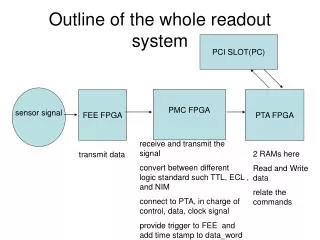
Outline of the whole readout system. PCI SLOT(PC). sensor signal. PMC FPGA. FEE FPGA. PTA FPGA. receive and transmit the signal convert between different logic standard such TTL, ECL , and NIM connect to PTA, in charge of control, data, clock signal

E N D
Outline of the whole readout system PCI SLOT(PC) sensor signal PMC FPGA FEE FPGA PTA FPGA receive and transmit the signal convert between different logic standard such TTL, ECL , and NIM connect to PTA, in charge of control, data, clock signal provide trigger to FEE and add time stamp to data_word 2 RAMs here Read and Write data relate the commands transmit data
MAPMT FEE_FPGA firmware compensate for trigger delay Delay_latch trigger D_latch D_push Push out 2+12 bit data during 12 clk parallel input128 bit parallel output 128 bit generate small range time_stamp BCO_clock Bco_counter C_latch
d_latch d_push=0 enable data latching; d_push=1 disable data latching; read_clk(16 Mhz) for all modules except bco_counter
delay_latching counter2<=counter2+1 //at rising edge of r_clk when c2=010 d_push=1 //pusing starts and latching stops when reset din(2:0)<=offset(2:0) // if offset=001 1clk delay //if offset =000 2 clk delay
d_push d_push=1 pushing data and disable latching using 12 clk to push a single event data (128 bits) with its time stamp to PMC/PTA pair: c6=0001 /dout<= time stamp and ctrl bits/ c6=0010-1100 /dout<=12bits event data+2bits ctrl(data_valid, data_ctrl)/ c6=1101 synchrs-> RESET
bco_counter &c_latch • bco clk and bco_counter generate time stamp (6 bits) • c_latch latch this stamp to push_data • bco_counter will also be RESET by the synchrs signal • RESET=synchrs+RS(mannually reset???)
PMC FPGA firmware • major modules data_latch: from output(either MAPMT or FPIX) to latch_out_up(11:0) latch_out_down(11:0) data_deserialize: latch_out_up(11:0)+latch_out_down(11:0) become : parallel(0)-parallel(24)
data format from FPIX • 24 bits data word 7 5 8 3 1=24 b23-b17 ROW b16-b12 COL. b11-b04 BCO b03-b01 ADC 1
data_latch has 4 modes: • one_line_latch • two_line_latch • four_line_latch • six_line_latch with respect to the 4 output configurations of FPIX (6 output pairs;4 output pairs;2 output pairs;1 output pair)
data_word format • after deserializing, add some bits to the data_word: FIRMWARE_TYPE(2) DATA(30) FIRMWARE_TYPE(1) DATA(29) FIRMWARE_TYPE(0) DATA(28) PLANE_ID(3) DATA(27) PLANE_ID(2) DATA(26) PLANE_ID(1) DATA(25) PLANE_ID(0) DATA(24) GND DATA(31)
PMC-PTA communication • JN1 & JN2 connect directly the PMC FPGA to PTA FPGA • JN2 connector is for data transmitting DATA_OUT(31:0) JN2_S0…JN2_S31 JN1 connector is for control singals and clock
Problems • front-end design is fine, but the back-end design could not be done, because some of the schematic symbols are missing of the PMC firmware, I can’t synthesize(netlist file),simulate or implement (bit file)the design… • what’s next?