Download
1 / 1
10 likes | 17 Views
The map is a suitable representation of the variation in performance across the substrate, since the distribution of those variants may be a hint as to their cause. The concept also comprises the package of data produced by modern wafer testing equipment which can be conveyed to equipment used for ensuring 'back-end' manufacturing processes.

E N D
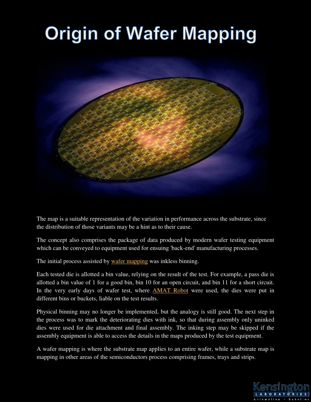
The map is a suitable representation of the variation in performance across the substrate, since the distribution of those variants may be a hint as to their cause. The concept also comprises the package of data produced by modern wafer testing equipment which can be conveyed to equipment used for ensuing 'back-end' manufacturing processes. The initial process assisted by wafer mapping was inkless binning. Each tested die is allotted a bin value, relying on the result of the test. For example, a pass die is allotted a bin value of 1 for a good bin, bin 10 for an open circuit, and bin 11 for a short circuit. In the very early days of wafer test, where AMAT Robot were used, the dies were put in different bins or buckets, liable on the test results. Physical binning may no longer be implemented, but the analogy is still good. The next step in the process was to mark the deteriorating dies with ink, so that during assembly only uninked dies were used for die attachment and final assembly. The inking step may be skipped if the assembly equipment is able to access the details in the maps produced by the test equipment. A wafer mapping is where the substrate map applies to an entire wafer, while a substrate map is mapping in other areas of the semiconductors process comprising frames, trays and strips.