Download
1 / 5
50 likes | 57 Views
The different dimension of features that are structured in the modern semiconductor manufacturing processes gets diminish without holding a significant impact over the manufacturing throughput.

E N D
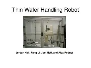
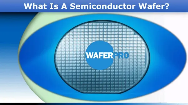
A Wafer Handling Automation with Alignment Accuracy for Semiconductor Applications When we talk about a typical semiconductor manufacturing, we see wafers transported in the cassettes by the guided vehicles and then further loaded or unloaded from the machines by a wafer handling robots. The different dimension of features that are structured in the modern semiconductor manufacturing processes gets diminish without holding a significant impact over the manufacturing throughput. Reluctantly, a gap gets emerge in the semiconductor field where the technologies are efficient in the in-line metrology. The recent advances in the fabrication of the microelectromechanical system have enabled AFM realization over a single MEMS chip. This MEMS-based AFM is proficient in scanning the little features at high speed over the micron-scale areas and is slight enough, incorporated into the manufacturing tools for the entire Nano scale measurement metrology
platforms. It comes with multi-scan probes that are to be performed over a wafer at the same time. Such low-cost devices lessen the setup time needed for the AFM metrology because they do not need to focus on a laser over the AFM cantilever tip. It is familiar with the ancient AFM systems and doesn't need the inspection wafer to be loaded into the considerable AFM system. However, it is essential to search for a spot over the wafer to dig and clear the points before measurement. Look improvements in the scanning area, and the throughput can be made possible by the MEMS-based AFMs via the incorporation of multiple AFM chips over a platform. The system that we are discussing here aims to lessen the AFM- based metrology setup by making the reputable alignment of the wafer handling automation over the low cost. It is to realize
the goal of the high throughput AFM based Nano scale metrology of the semiconductor wafers. This metrology system is capable of the silicon wafers' in-line metrology after lithography or carving steps in the semiconductor manufacturing process. For now, it is impossible to measure the non-scale features in-line with the semiconductor manufacturing process since the methodologies are too slow for the in-line process measurements. So, in the semiconductor manufacturing process, the wafers are taken out from the manufacturing line every hour and further analyzed with the time-intensive methods like scanning electron microscopy. It means that a defective wafer can get through the manufacturing process before the occurrence of any error. Moreover, in-line metrology is visualized by precision alignment methods. It will help you identify the errors very abruptly within the manufacturing process and lessen the semiconductor manufacturing scrap rate. Now, what you need to know that the transportation of the wafer front end between the semiconductor manufacturing can be attained by the wafer handling robots. The wafer handling automation is dependent on the compliance arm for the robot assembly. The SCARA wafer handling robots gets processed in the horizontal work plane and vertical work plane in 1DOF and 3DOF. So, these wafer handling robots can hold up
the throughputs of up to 350 wafers per hour with the positioning repeatability of 100 um. Do you know that the wafer's optical alignment is acquired by rotating the wafer, and the optical sensor's help to detect the wafer fiat's location? The wafers can be easily aligned concerning the tool of metrology. Do you know that the optical mean achieves the active wafer alignment? You must know that the most known optical wafer alignment method indulges the patterning alignment that marks over a wafer substrate. Such alignments are seen beneath the microscope, which contains a matching mark. Alignment can be further achieved when the two marks get in line with each other simultaneously. The submicron repeatability has been visualized with the help of this same method. The manual wafer registration through the optical alignment is a very time-consuming process that is not
practical for the in-line metrology applications. The automated optical alignment systems use the robotic arms and the vision systems to attain the submicron wafer alignment. But you must know that it is costly to implement in the metrology systems which don't have imaging optics and the closed-loop controls for the wafer placement. If we talk about the advanced optical alignment system, it relies on the marks' interference patterns and can sub 20 nm wafer alignment. Infact, these systems are implemented in the multimillion-dollar nano-manufacturing tools. It needs good wafer alignment repeatability as the cost and resolution are higher than the general-purpose semiconductor metrology platform. Don’t delay to check out the Kensington Laboratories that provides the wafer handling automation to the industries at a modest rate. Source Link: https://bit.ly/3kDL2y0