Download
1 / 46
530 likes | 683 Views
Introduction to IC Design. Tsung-Chu Huang ( 黃宗柱 ) Department of Electronic Eng. Chong Chou Institute of Tech. Email: tch@dragon.ccut.edu.tw 2003/10/13. CMOS Process Tech. Si Semiconductor Technology Basic CMOS Technology CMOS Process Layout Design Rules Latchup Effect

E N D
Introduction to IC Design Tsung-Chu Huang (黃宗柱) Department of Electronic Eng. Chong Chou Institute of Tech. Email: tch@dragon.ccut.edu.tw 2003/10/13
CMOS Process Tech • Si Semiconductor Technology • Basic CMOS Technology • CMOS Process • Layout Design Rules • Latchup Effect • Extractor & DRC • An n-Well CMOS Process Flow • CIC Tape-In Flow & Tutorial
CMOS Process Tech • Oxidation (氧化) • Epitaxy (磊晶) • Deposition (沉積) • Implantation (植入) • Diffusion (擴散)
Wafer Processing mm/min 1425°C Czochralski’s Method
Wafer Treatments • Grinding • Slicing • Lapping • Etching • Polishing • Cleaning • Inspection
Wafer Size 16” 12” 8” 6” 3” 1970 1980 1990 2000 2010
Oxidation Wet Dry O2 O2 1200°C H2O 900°C
Chemical Vapor Deposition Impurity Vapor (e.g., Ga, In) P Substrate
Epitaxy Si Vapor Single Crystal
Diffusion Impurity
Iron Implantation Impurity Iron • Previously used to adjust the threshold voltage; • Currently usually used to be active region.
Common Material Used As Masks • Photoresist • Polysilicon • Silicon Dioxide • Silicon Nitride
Masking using PR UV Solvant 1 Photo Masking Coating with a PR Sloved after the process using the mask Self-Align: if the rest mask is also a useful layer.
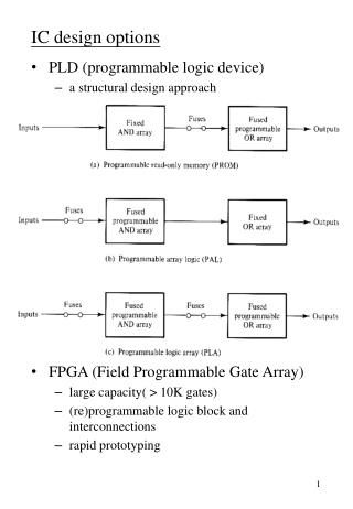
Basic CMOS Technology • N-Well Process • P-Well Process • Twin-Well (Twin-Tub) Process • Silicon on Insulator
Major IC Manufacture Flow • 電路設計 • 〈IC design〉 • 晶圓加工 • 〈wafer fabrication, FAB〉 • 封裝 • 〈packaging〉 • 測試 • 〈test〉
A Detailed MOS Process Courtesy of Chuang, “VLSI Technology,” ISBN:957-584-327-4 .
電晶體簡化佈局流程 決定“閘”(Gate)的長與寬 寬 W 長 L 薄氧化層 Thinox 決定工作區域(Active Region) 上視圖 剖面圖
電晶體簡化佈局流程 遮照 Mask 厚氧化層 Thick Oxide 剖面圖
電晶體簡化佈局流程 遮罩 Mask 剖面圖
電晶體簡化佈局流程 擴散(Diffusion) 或 離子植入(Implant)區 上視圖 剖面圖
電晶體簡化佈局流程 上視圖 決定電晶體是 P 或 N 型
以一個Not gate加以說明 上視圖 P型電晶體 N型電晶體 電子移動率Mobility, m ~ 1 : 2.6 通常,為了讓Noise margin平衡,或使NOT閘的臨界電壓折中: P型電晶體的W/L常為N型的2到3倍!
N-Well製程 金屬, Al 或 Cu, Metal P+ P+ N+ N+ 上視圖 N+ Imp, 高濃度N型植入 P+ Imp, 高濃度P型植入 剖面圖 N-Bulk P-Substrate
N-Well製程 上視圖 剖面圖 N Well
Latch-up Effect in n-Well Process Vss IN 上視圖 OUT Vdd 剖面圖 Latch up ! 正回授鎖死而燒毀!
Preventing Latch-up • Using Twin-Well (雙井製程) • Evolved in DRC • 每個N-Well要有N-型Contact接Vdd • 近Source-gate(源極) • 一般5~10個電晶體最少加一個Well Contact • 有的Rule甚至要求一個電晶體加一個Well contact
Contact Basic 4 Layers:
Via Metal 2 Metal 1 The widths of a via or contact are much sensitive to the process so that they are usually optimized to a constant, say 0.4um in 0.35um technology.
Local Interconnections Diffusion as interconnection: • Diffusion: < 1 Transistor • N-Well: < 1~5 Transistors • Polysilicon: 1~5 Transistors
SAlicide Silicide: a refractory metal, e.g., Si+Ta, Rs~1 Polysilicon Process Polysilicon: a multi-crystal semiconductor, Rs~10 Silicide Process Polycide Process Self-Aligned Polycide Process
Thin Film Process SOI Process Thin Film Transistor (TFT) Hi-density memory, Flat-Panel Display
Silicon on Insulator (SOI) Transistor(s) Without Inter-leakage Transistor(s) Without Inter-leakage P bulk N bulk Sapphire (藍寶石)
Design Rule Check (DRC) • Geometrical • X-Y Plane: Single-Layer Layout • Z Plane: Interactions btw Layers • ERC • Electrical Rule Check • Custom Rules
Scaling l 1 C=K C=lK • Linear Scaling
Scaling l 1 A=K A=l2K • First Order Scaling
Basic Categories of Rules • Micron (m) Rules • Listing all min. feature sizes in m’s • Re-listing is required after scaling. • Lambda (l) Rules • The min. active width = 1 l (mm). • Linear Scaling by l (l/m Rule). • First Order Scaling. • Must be modified in another range.
Basic Parameters in DRC Spacing Extend Width
Some Related Terminology Circuit Extractor Logic Extractor
Basic CIC Tape-In Flow Customer Transaction Extract Designer Layout Engineer Frontend HDL, Sch Netlist… HDL, Sch Netlist… LVS Simulation Backend Foundry DRC Tape-In Tape-Out
Reverse Engineering (RE) • Category • Mechanism • Software: database, programming • VLSI: layout • Purpose: • Failure inspection • Amoral hack, referring • Illegal stealing (duplication)
VLSI RE Flow • Unpacking • Chemical Metal Polishing (CMP) • Photographing • Inspection • Schematic • Simulation & Verification
Reversing Rule Check Layout DRC LVS Layout DRC Schematic Inspection Simulation Forward Engineering: Schematic Reverse Engineering: Photo