Download
1 / 38
510 likes | 1.02k Views
IC DESIGN ,. , Presented by MURALI.A. AGENDA. OVERVIEW OF ELECTRONIC DESIGN VLSI DESIGN FLOW FRONT END DESIGN BACK END DESIGN FPGA-FLOW FPGA vs ASIC. Common Products. Communication Mobiles / Telephones / RF / Satellite Video Audio TV / Audio players / Video players

E N D
IC DESIGN , , Presented by MURALI.A
AGENDA • OVERVIEW OF ELECTRONIC DESIGN • VLSI DESIGN FLOW • FRONT END DESIGN • BACK END DESIGN • FPGA-FLOW • FPGA vs ASIC MURALI.A, FACULTY DEPT OF ECE, LIET HYDERABAD
Common Products • Communication • Mobiles / Telephones / RF / Satellite • Video Audio • TV / Audio players / Video players • Computers • PC / Laptop / PDAs / Memory • Networking • Switches / Routers / Wi-Fi • Print • Printers / Fax / Scanners • Cameras • Video camera / Still cameras • Video Gaming • Xbox / PlayStation MURALI.A, FACULTY DEPT OF ECE, LIET HYDERABAD
Industries • Consumer • Automobile • Sensors / Control • Defense • Military / Air Force / Navel • Space & Avionics • Satellites / Airlines/ GPS • Industrial • Automation MURALI.A, FACULTY DEPT OF ECE, LIET HYDERABAD
Applications/Solutions/User-Interface Application software Operating Systems Device Drivers, Memory Managers Multi Threading Low Level Software Board Design Power supply Integration Hardware Integration Generic ICs like Microprocessors & RAMs Application Specific ICs (ASICs) Programmable Chips (FPGA/EPLD) Chip Design Product Development MURALI.A, FACULTY DEPT OF ECE, LIET HYDERABAD
Product Concept MURALI.A, FACULTY DEPT OF ECE, LIET HYDERABAD
COMPONENTS MURALI.A, FACULTY DEPT OF ECE, LIET HYDERABAD
PRINTED CIRCUIT BOARD MURALI.A, FACULTY DEPT OF ECE, LIET HYDERABAD
Hardware MURALI.A, FACULTY DEPT OF ECE, LIET HYDERABAD
INTEGRATED CIRCUITS – ASIC/FPGA MURALI.A, FACULTY DEPT OF ECE, LIET HYDERABAD
Hardware Development Electronics PCB ASIC Layout Design Make Front End Back End Fab Design Verification MURALI.A, FACULTY DEPT OF ECE, LIET HYDERABAD
VLSI TECHNOLOGY MURALI.A, FACULTY DEPT OF ECE, LIET HYDERABAD
WHAT IS VLSI ? • VLSI stands for • "Very Large Scale Integration" • VLSI is the process of integrating millions of transistors on tiny silicon chips to perform a multiple of logic operations with timings. MURALI.A, FACULTY DEPT OF ECE, LIET HYDERABAD
WHY WE NEED VLSI ? • To Implant a full system on a single chip • To Increase the complexity of the IC(no. of Transistors per chip) • To minimize the size of an IC or System • To Increase the processing speed of a System • To reduce power consumed by a system • VLSI family i.e. PLD’s, FPGA’s, ASIC’s along with EDA Tools have changed the VLSI Design scenario. MURALI.A, FACULTY DEPT OF ECE, LIET HYDERABAD
Scope of VLSI Engineers • Design engineer. • Product engineer. • Test engineer. • Application engineer. • Process engineer. • Packaging engineer. • CAD engineer. MURALI.A, FACULTY DEPT OF ECE, LIET HYDERABAD
VLSI Design Process • The major design steps are different levels of Abstractions. • Problem specification • Architecture definition • Functional design • Logic design • Physical design • packaging MURALI.A, FACULTY DEPT OF ECE, LIET HYDERABAD
Physical Design • The conversion of the net list into its geometrical representation. • Circuit partitioning • Floor planning and Placement • Routing • Layout design • Extraction and Verification MURALI.A, FACULTY DEPT OF ECE, LIET HYDERABAD
What jobs does an VLSI Engineers do? • Design engineer. • Product engineer. • Test engineer. • Application engineer. • Process engineer. • Packaging engineer. • CAD engineer. MURALI.A, FACULTY DEPT OF ECE, LIET HYDERABAD
IC Products • Processors • CPU, DSP, Controllers • Memory chips • RAM, ROM, EEPROM • Analog • Mobile communication,audio/video processing • Programmable • PLA, FPGA • Embedded systems • Used in cars, factories • Network cards • System-on-chip (SoC) MURALI.A, FACULTY DEPT OF ECE, LIET HYDERABAD
Microelectronics-Technology growth • MOORE’S LAW • The CMOS technology has followed Moore’s law for more than20 years. • Moore’s Law : “The transistor density on IC doubles every 18 months” • Analysts predict continuation of current path until 2014 and beyond • By the year 2010 one IC will provide as much computing power as 200 pentium II’s running at 3 GHZ. • Following is the growth of micron technology. MURALI.A, FACULTY DEPT OF ECE, LIET HYDERABAD
MOS Technology Trends MURALI.A, FACULTY DEPT OF ECE, LIET HYDERABAD
SSI / MSI A few thousand transistors 1960s LSI Processors, 1Kb Memory 1970s VLSI Millions of transistors Growth of EDA/Computing VHDL/Verilog 1980s Programmable Chips FPGA/EPLD/CPLD Process Improvements Cost/Speed/Low-Power 180nm / 130nm 1990s New Applications Mobile / Consumer / Industrial SOPCs Multi million gate High Speed ULSI Billions of transistors Multi Core processors 64-bit processors System-On-Chip DRAMs / Flash 90nm / 60nm / 28nm 21st Century Entertainment Video / Gaming / Graphics Smart Phones FPGAs Application Specific Designs High Performance Computing Integrated Circuits
INTEL-PROCESSORS– An Evolution.. MURALI.A, FACULTY DEPT OF ECE, LIET HYDERABAD
VLSI DESIGN FLOW MURALI.A, FACULTY DEPT OF ECE, LIET HYDERABAD
Specifications Design Verification Verilog VHDL C/Perl SysVerilog Specman Verilog/VHDL Simulation Models Synthesis Functional Simulation Modelsim VCS NCSim Libs / Const Libs / Const Pre Route STA Clock Tree Synthesis Placement Routing Netlist - SDF Formal Verification Post Route STA Gate Level Simulations MURALI.A, FACULTY DEPT OF ECE, LIET HYDERABAD
Logical Physical ASIC Design Flow Specifications Functional Simulation Design Entry Logic Synthesis Pre-Layout Simulation Static Timing Analysis System partitioning and Floor-planning Post-Layout Simulation Placement and Routing Physical Verification Fab proto type and Testing Production MURALI.A, FACULTY DEPT OF ECE, LIET HYDERABAD
FPGA Design Flow Design entry Schematics HDL simulation synthesis mapping Place & route Configuration MURALI.A, FACULTY DEPT OF ECE, LIET HYDERABAD
Fusing FPGA using JTAG : Bit file configuration MURALI.A, FACULTY DEPT OF ECE, LIET HYDERABAD
FPGA Prototype Board (Example) Diagnostics S/w ROM CPU DMA CNTRL (FPGA) DRAM CNTRL (FPGA) DRAM UART (FPGA) RS-232 CNTRL SRAM DATA ADDRESS Cfg PROM MURALI.A, FACULTY DEPT OF ECE, LIET HYDERABAD
FPGA’s on PCB’s MURALI.A, FACULTY DEPT OF ECE, LIET HYDERABAD
Suppliers of Programmable Logic Devices • Xilinx • Altera • Cypress • Lattice • Philips • Vantis • Cirrus Logic • Quick Logic • Actel • Atmel • Lucent MURALI.A, FACULTY DEPT OF ECE, LIET HYDERABAD
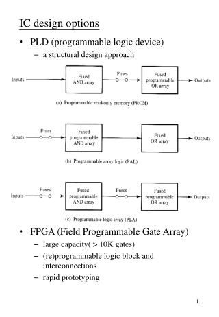
Different kinds of programmable logic devices available today • Major types : i. Simple Programmable Logic Devices (SPLDs) ii. Complex Programmable Logic Devices (CPLDs) iii.Field Programmable Gate Arrays (FPGAs) MURALI.A, FACULTY DEPT OF ECE, LIET HYDERABAD
SPLDs & CPLDs • SPLDs are also known as: • PAL (Programmable Array Logic, Vantis) • GAL (Generic Array Logic, Lattice) • PLA (Programmable Logic Array) • PLD (Programmable Logic Device) • SPLDs are the smallest and consequently the least-expensive form of programmable logic.It Contains 4 to 22 macrocells and can typically replace a few 7400-series TTL devices • Array of SPLDs can say as CPLDs MURALI.A, FACULTY DEPT OF ECE, LIET HYDERABAD
Spartan -3E Starter Kit : Features • Xilinx Devices: • Spartan-3E FPGA (XC3S500E-4FG320C) • CoolRunner™-II CPLD (XC2C64A-5VQ44C) • Platform Flash (XCF04S-VO20C) • Clocks: 50 MHz crystal clock oscillator • Memory: • 128 Mbit Parallel Flash • 16 Mbit SPI Flash • 64 MByte DDR SDRAM • Connectors and Interfaces: • Ethernet 10/100 Phy • JTAG USB download • Two 9-pin RS-232 serial port • PS/2- style mouse/keyboard port, rotary Three 6-pin expansion connectors • Display: 16 character - 2 Line LCD MURALI.A, FACULTY DEPT OF ECE, LIET HYDERABAD
Thank - U MURALI.A, FACULTY DEPT OF ECE, LIET HYDERABAD