Download
1 / 20
200 likes | 325 Views
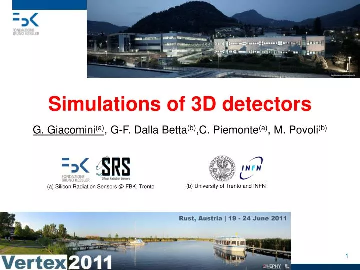
Simulations of 3D detectors. G. Giacomini (a) , G-F. Dalla Betta (b) ,C. Piemonte (a) , M. Povoli (b). (a) Silicon Radiation Sensors @ FBK, Trento. (b) University of Trento and INFN. Outline 3D sensors: properties, state-of-the-art and technology @ FBK

E N D
Simulations of 3D detectors G. Giacomini(a), G-F. Dalla Betta(b),C. Piemonte(a), M. Povoli(b) (a) Silicon Radiation Sensors @ FBK, Trento (b) University of Trento and INFN
Outline • 3D sensors: properties, state-of-the-art and technology @ FBK • TCAD simulations for 3D sensors: peculiarities • Selected simulations : • C-V depletion map • SLIM edge • Signals from test beam charge sharing • Multiplication effect (?)
3D detectors ADVANTAGES: • Electrode distance and active substrate thickness decoupled: - Low depletion voltage - Short Collection distance - Smaller trapping probability after irradiation High radiation hardness • Active edges: - Dead area reduced up to few microns from the edge First proposed by S. Parker et. al. in NIMA 395 (1997), 328 Best result: 66% of the original signal after Fluence = 8.8x1015 cm-2 1-MeV neq. @ 100 V DISADVANTAGES: • Non uniform response due to electrodes • Complicated technology • Higher capacitance (X3) with respect to planar C. Da Via et. al.: NIMA 604 (2009) 504
Latest 3D technology @ FBK ~ 200-mm P-type substrate, n-junction columns insulated by p-spray NOT FULL PASSING COLUMNS • fabrication process reasonably simple • proved good performance up to irradiation fuence of 1015 neq/cm2 (even with non optimized gap “d”) but - column depth difficult to control and to reproduce - insufficient performance after very large irradiation fluences if “d” is too large n+ col p-spray p+ col FULL PASSING COLUMNS • Column depth = wafer thickness • More complicated process back patterned From G.-F. Dalla Betta, IEEE NSS 2010, N15-3
The TCAD Simulator Simulations presented are performed with Synopsis Sentaurus (former ISE-TCAD) 1D, 2D and 3D simulator solving physical equations (Poisson, drift, diffusion, …) Static and dynamics measurements Wafer layout and fabrication Process and device simulation Interpretation of measurements with simulations
TCAD Simulator for 3D Simulation for understanding the properties of different kind of 3D sensors have been the subject of many papers: • Parker et al.: “3D – A proposed new architecture for solid-state radiation detectors” NIM A395 (1997) 328-343 • Piemonte et al.: “Development of 3D detectors featuring columnar electrodes of the same doping type” NIMA 541 (2008) 441 • Zoboli et al.: “Double-Sided, Double-Type-Column 3-D Detectors: Design, Fabrication, and Technology Evaluation” TNS 55 (2008) 2775 • Pennicard et al.: “Simulations of radiation-damaged 3D detectors for the Super-LHC” NIM A 592 (2008) 16–25 For the different technologies, we studied both static (I-V and C-V) and dynamic behavior (signals from optical and high-energy particles).
Peculiarity of 3D detector simulations For a 3D detector, we must use 3D simulations, since properties varies with depth. high number of nodes, long CPU time, … On the other hand, structures may show regular pattern and the elementary cell can be quite small. Example of 3D layout Simulated structure = elementary cell Upper surface 80 mm Bottom surface METAL GRID p+ column n+ column
Example 1. C-V simulation Capacitance vs Vbias of an array of n - columns vs p - columns (back) of a 3D diode. C-V curve does not saturate for Vbias > Vdepl, like in a standard planar Diode (1D approx), To understand this effect we simulate: • elementary cell. • p-spray profile measured with SIMS and inserted in simulation. From G.-F. Dalla Betta, IEEE NSS 2010, N15-3
Example 1. C-V simulation Capacitance vs Vbias of an array of n+columns vs p+columns (back) of a 3D diode. C-V curve does not saturate for Vbias > Vdepl, like in a standard planar Diode (1D approx), To understand this effect we simulate: • elementary cell. • p-spray profile measured with SIMS and inserted in simulation. From G.-F. Dalla Betta, IEEE NSS 2010, N15-3
C-V simulation Hole concentration vs Vbias 1V 2V 3V 4V 6V= Vdepletion 8V 10V • At mid-substrate, (hole) depletion already @ Vbias = 6 V. • Important capacitance contribution from p-spray which is slowly depleting also at higher voltages.
Example 2. SLIM EDGE Problem: ATLAS IBL requires a max. dead layer of 450 mm along Z for FE-I4 read-out. 50 mm p (ohmic) columns Standard Active edge difficult to implement because of support wafer SLIM EDGE • Multiple Ohmic (p-col.) fence termination • Dead area can be as low as~ 200 mm 250 mm 200 mm SCRIBE LINE Does it work? n (junction) columns From G. Giacomini, 6th “Trento” WS on 3D and p-type detectors, March 2011
SLIM EDGE The scribe line is simulated as a low-t region: if depletion region touches it HIGH current!! 80 mm Vbias = 30 V p+ (ohmic) columns Hole density (cm-3) SLICE AT Y = 100 mm 80 mm Scribe line: Very Low t Domain of simulation Vbias = 30 V 250 mm n+ (junction) columns SCRIBE LINE Even for Vbias >> Vdepl, depletion region hardly extends beyond second p-col row.
SLIM EDGE 5th cut Experimentally, it works: Dicing away one row at a time and measuring the I-V, It is shown that one row of ohmic holes is sufficient to “stop” the depletion region 3th cut 6th cut 40 mm 1st cut p+ (ohmic) columns n+ (junction) columns
Example 3. Signal from irradiated devices Old FBK 3D sensor, not full passing columns proton irradiated @ 1e15 neq/cm2 Collimated Sr source Qmean (fC)) Vbias (V) C. Gallrap et al., "Characterisation of irradiated FBK sensors". ATLAS 3D Sensor General Meeting, CERN, October 26, 2010. We want to reproduce this “not intuitive” trend: 3D is “ideal” only in the columnar overlapping, while only a simulation can predict the collection of electrons generated below the column fluence dependent
Signal from irradiated devices X Bulk simulated according to “Perugia” model: Petasecca TNS 53 (2006) 2971; Pennicard NIM A 592 (2008) 16–25 N-column 2 To simulate the charge sharing: double the elementary cell m.i.p. crossing the bulk simulated with uniform charge release (80 pairs/mm) and with different track angles N-column1 Y z P-column
Signal from irradiated devices Column N1- signals Column N2- signals Integrals of currents ( = total collected Charge) saturate before 20 ns (no ballistic deficit for ATLAS ROC) and at a value exceeding the threshold of 3200 e- (0.5 fC) (ATLAS threshold)
Signal from irradiated devices Simulating Cluster size 1 vs Bias voltage and Simulating Cluster size 2 vs Bias voltage (for few impinging points) and weighting the simulated results with geometrical/experimental considerations, we get a simulated curve of the total charge vs Vbias, which fits well the irradiation experiment results.
Example 4. Multiplication effects work in progress! In an irradiated p-on-n strip sensor (F= 1e15 neq/cm2), already at ~ 150 V, CCE vs V plots shows an anomalous increase of IV and CCE-V. It is believed that this effect comes from impact ionization A. Zoboli, IEEE NSS 2008, N34-4
Multiplication effects work in progress! Simulating multiplication with: - impact ON - effective bulk doping/oxide charge no multiplication - impact ON and - traps from “Perugia” model MULTIPLICATION close to the measured one 60 irradiated – F=1e15 neq strip sensor p-on-n charge 50 Simul. Leakage Simul. Charge W traps Simul. Charge W/o traps Measured Charge 40 Current (mA) Collected Charge (fC) F = 1e15 neq/cm2 30 20 p-col 10 Vbias n-substrate n-col
CONCLUSIONS Simulations of 3D are fundamental because of the complexity of the device. Different geometries & different Models must be chosen according to the simulation We showed that simulations are useful both at the design stage as well as to understand peculiar effects.