Download

1 / 34
380 likes | 948 Views
Lecture 7 Diode Circuit Models and Applications. 1. i. i. 3. Graphical analysis using load-line method. i. Linear Circuit. I and V must satisfy both the linear And non-linear circuit equations. +. -. Nonlinear element. For the linear circuit.

E N D
i i 3. Graphical analysis using load-line method. i Linear Circuit I and V must satisfy both the linear And non-linear circuit equations + - Nonlinear element For the linear circuit Finding Thevenin or Norton equivalent of the linear circuit +
Load-Line Analysis (Example) Problem: Find Q-point Given data:V=10 V, R=10kW. Analysis: To define the load line we use, VD= 0 VD= 5 V, ID =0.5 mA These points and the resulting load line are plotted.Q-point is given by intersection of load line and diode characteristic: Q-point = (0.95 mA, 0.6 V) 3
4. Analysis using Mathematical Model for Diode Ideal Diode
i ISC =VOC/R ib i ia v va VOC=Vth Iterative Method based on Mathematical Model i Linear Circuit I and V must satisfy both the linear And non-linear circuit equations + Exponential diode equation - Nonlinear element Linear circuit equation
Example: Analysis using Mathematical Model for Diode Problem: Find Q-point for given diode characteristic. Given data: IS =10-13 A, n=1, VT =0.0025 V Analysis: is load line, given by a transcendental equation. A numerical answer can be found by using iterative method. Use the technique in the previous slide Q-point = ( 0.9426 mA, 0.5742 V) Since, usually we don’t have accurate saturation current and significant tolerances for sources and passive components, we need answers precise up to only 2or 3 significant digits. 6
Diode Circuits • After we have studied in detail the physics of a diode, it is time to study its behavior as a circuit element and its many applications.
Diode’s Action in The Black Box (Ideal Diode) • The diode behaves as a short circuit during the positive half cycle (voltage across it tends to exceed zero), and an open circuit during the negative half cycle (voltage across it is less than zero).
Diode’s application: Limiter • The purpose of a limiter is to force the output to remain below certain value. • In a), the addition of a 1 V battery forces the diode to turn on after V1 has become greater than 1 V.
Limiter: When Battery Varies • An interesting case occurs when VB (battery) varies. • Rectification fails if VB is greater than the input amplitude.
Input/Output Characteristics with Ideal and Constant-Voltage Models
Input/Output Characteristics with a Constant-Voltage Model • When using a constant-voltage model, the voltage drop across the diode is no longer zero but Vd,on when it conducts.
Another Constant-Voltage Model Example • In this example, since Vin is connected to the cathode, the diode conducts when Vin is very negative. • The break point where the slope changes is when the current across R1 is equal to the current across R2. CH3 Diode Circuits
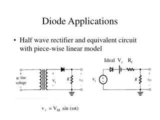
2. Rectifier Circuits • Basic rectifier converts an ac voltage to a pulsating dc voltage. • A filter then eliminates ac components of the waveform to produce a nearly constant dc voltage output. • Rectifier circuits are used in virtually all electronic devices to convert the 120 V-60 Hz ac power line source to the dc voltages required for operation of the electronic device. • In rectifier circuits, the diode state changes with time and a given piecewise linear model is valid only for a certain time interval. 15
Half-Wave Rectifier Circuit with Resistive Load For positive half-cycle of input, source forces positive current through diode, diode is on, vo = vs. During negative half cycle, negative current can’t exist in diode, diode is off, current in resistor is zero and vo =0 . 16
Half-Wave Rectifier Circuit with Resistive Load (contd.) Using constant voltage model CVD model, during on state of diode vo =(VP sinwt)- Vd,on. Output voltage is zero when diode is off. Often a step-down transformer is used to convert 120 V-60 Hz voltage available from power line to desired ac voltage level as shown. Time-varying components in circuit output are removed using filter capacitor. 17
Peak inverse voltage (PIV) Half-Wave Rectifier Circuit with Resistive Load (contd.) Select a diode that has at least 50% higher PIV 18
Half-Wave Rectifier Circuit with RC Load As input voltage rises during first quarter cycle, diode is on and capacitor (initially discharged) charges up to peak value of input voltage. At peak of input, diode current tries to reverse, diode cuts off, capacitor discharges exponentially through R. Discharge continues till input voltage exceeds output voltage which occurs near peak of next cycle. Process then repeats once every cycle. This circuit can be used to generate negative output voltage if the top plate of capacitor is grounded instead of bottom plate. In this case, Vdc = -(VP - Von) 19
Equation (1) Finding the Ripple Voltage
Equation (2) Conduction Angle
Half-Wave Rectifier Circuit with RC Load (contd.) Output voltage is not constant as in ideal peak detector, but has ripple voltageVr. Diode conducts for a short time DT called conduction interval during each cycle and its angular equivalent is called conduction angleθc. 22
Half-Wave Rectifier Analysis: Example Problem: Find dc output voltage, output current, ripple voltage, conduction interval, conduction angle. Given data: secondary voltage Vrms 12.6 (60 Hz), R= 15 W, C= 25,000 mF, Vd = 1 V Analysis: Using discharge interval T=1/60 s, 23
Peak Inverse Voltage Rating Peak inverse voltage (PIV) rating of the rectifier diode gives the breakdown voltage. When diode is off, reverse-bias across diode is Vdc - vs. When vs reaches negative peak, PIV value corresponds to minimum value of breakdown voltage for rectifier diode. 24
Peak Diode Current In rectifiers, nonzero current exists in diode for only a very small fraction of period T, yet an almost constant dc current flows out of filter capacitor to load. Total charge lost from capacitor in each cycle is replenished by diode during short conduction interval causing high peak diode currents. 25
Full-Wave Rectifiers Full-wave rectifiers cut capacitor discharge time in half and require half the filter capacitance to achieve given ripple voltage. All specifications are same as for half-wave rectifiers. Reversing polarity of diodes gives a full-wave rectifier with negative output voltage. 28
Full-Wave RectifiersTransformer-Based PIV = 2vs-vD 29
Full-Wave Bridge Rectification Requirement for a center-tapped transformer in the full-wave rectifier is eliminated through use of 2 extra diodes.All other specifications are same as for a half-wave rectifier except PIV. 30
Full-Wave Bridge Rectification PIV = vs-vD 31
Rectifier Topology Comparison • Filter capacitor is a major factor in determining cost, size and weight in design of rectifiers. • For given ripple voltage, full-wave rectifier requires half the filter capacitance as that in half-wave rectifier. Reduced peak current can reduce heat dissipation in diodes. Benefits of full-wave rectification outweigh increased expenses and circuit complexity (a extra diode and center-tapped transformer). • Bridge rectifier eliminates center-tapped transformer, PIV rating of diodes is reduced. Cost of extra diodes is negligible. 32
Peak Detector Circuit(Clamping circuit) As input voltage rises, diode is on and capacitor (initially discharged) charges up to input voltage minus the diode voltage drop. At peak of input, diode current tries to reverse, diode cuts off, capacitor has no discharge path and retains constant voltage providing constant output voltage Vdc = VP – Vd,on. 34