Download
1 / 34
340 likes | 532 Views
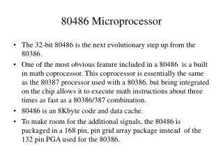
80486 Microprocessor. The 32-bit 80486 is the next evolutionary step up from the 80386.

E N D
80486 Microprocessor • The 32-bit 80486 is the next evolutionary step up from the 80386. • One of the most obvious feature included in a 80486 is a built in math coprocessor. This coprocessor is essentially the same as the 80387 processor used with a 80386, but being integrated on the chip allows it to execute math instructions about three times as fast as a 80386/387 combination. • 80486 is an 8Kbyte code and data cache. • To make room for the additional signals, the 80486 is packaged in a 168 pin, pin grid array package instead of the 132 pin PGA used for the 80386.
Pin Definitions • A 31-A2: Address outputs A31-A2 provide the memory and I/O with the address during normal operation. During a cache line invalidation A31-A4 are used to drive the microprocessor. _____ • A20M3:The address bit 20 mask causes the 80486 to wrap its address around from location 000FFFFFH to 00000000H as in 8086. This provides a memory system that functions like the 1M byte real memory system in the 8086 processors. ____ • ADS : The address data strobe become logic zero to indicate that the address bus contains a valid memory address. Next page
AHOLD: The address hold input causes the microprocessor to place its address bus connections at their high-impedance state, with the remainder of the buses staying active. It is often used by another bus master to gain access for a cache invalidation cycle. BREQ: This bus request output indicates that the 486 has generated an internal bus request. ____ ____ • BE3-BE0: Byte enable outputs select a bank of the memory system when information is transferred between the microprocessor and its memory and I/O. The BE3 signal enables D31 – D24 , BE2 enables D23-D16, BE1 enables D15 – D8 and BE0 enables D7-D0. Next page
____ • BLAST: The burst last output shows that the burst bus cycle is complete on the next activation of BRDY# signal. _____ • BOFF : The Back-off input causes the microprocessor to place its buses at their high impedance state during the next cycle. The microprocessor remains in the bus hold state until the BOFF# pin is placed at a logic 1 level. • NMI : The non-maskable interrupt input requests a type 2 interrupt. Next page
____ • BRDY : The burst ready input is used to signal the microprocessor that a burst cycle is complete. ____ • KEN : The cache enable input causes the current bus to be stored in the internal. _____ • LOCK : The lock output becomes a logic 0 for any instruction that is prefixed with the lock prefix. __ • W / R : current bus cycle is either a read or a write. Next page
______ • IGNNE : The ignore numeric error input causes the coprocessor to ignore floating point error and to continue processing data. The signal does not affect the state of the FERR pin. ______ • FLUSH : The cache flush input forces the microprocessor to erase the contents of its 8K byte internal cache. _____ • EADS: The external address strobe input is used with AHOLD to signal that an external address is used to perform a cache invalidation cycle. Next page
_____ • FERR : The floating point error output indicates that the floating point coprocessor has detected an error condition. It is used to maintain compatibility with DOS software. ___ • BS8: The bus size 8, input causes the 80486 to structure itself with an 8-bit data bus to access byte-wide memory and I/O components. ____ • BS16: The bus size 16, input causes the 80486 to structure itself with an 16-bit data bus to access word-wide memory and I/O components.
_____ • PCHK : The parity check output indicates that a parity error was detected during a read operation on the DP3 – DP0 pin. ______ • PLOCK : The pseudo-lock output indicates that current operation requires more than one bus cycle to perform. This signal becomes a logic 0 for arithmetic coprocessor operations that access 64 or 80 bit memory data. • PWT: The page write through output indicates the state of the PWT attribute bit in the page table entry or the page directory entry. Next page
____ • RDY : The ready input indicates that a non-burst bus cycle is complete. The RDY signal must be returned or the microprocessor places wait states into its timing until RDY is asserted. __ __ • M / IO : Memory / IO defines whether the address bus contains a memory address or an I/O port number. It is also combined with the W/ R signal to generate memory and I/O read and write control signals.
80486 Signal Group • The 80486 data bus, address bus, byte enable, ADS#, RDY#, INTR, RESET, NMI, M/IO#, D/C#, W/R#, LOCK#, HOLD, HLDA and BS16# signals function as we described for 80386. • The 80486 requires 1 clock instead of 2 clock required by 80386. • A new signal group on the 486 is the PARITY group DP0-DP3 and PCHK#. • These signals allow the 80486 to implement parity detection / generation for memory reads and memory writes. • During a memory write operation, the 80486 generates an even parity bit for each byte and outputs these bits on the DP0-DP3 lines. Next page
These bits will store in a separate parity memory bank. • During a read operation the stored parity bits will be read from the parity memory and applied to the DP0-DP3 pins. • The 80486 checks the parities of the data bytes read and compares them with the DP0-DP3 signals. If a parity error is found, the 80486 asserts the PCHK# signal. • Another new signals group consists of the BURST ready signal BRDY# and BURST last signal BLAST#. • These signals are used to control burst-mode memory reads and writes. Next page
A normal 80486 memory read operation to read a line into the cache requires 2 clock cycles. However, if a series of reads is being done from successive memory locations, the reads can be done in burst mode with only 1 clock cycle per read. • To start the process the 80486 sends out the first address and asserts the BLAST# signal high. When the external DRAM controller has the first data bus, it asserts the BRDY# signal. • The 80486 reads the data word and outputs the next address. Since the data words are at successive addresses, only the lower address bits need to be changed. If the DRAM controller is operating in the page or the static column modes then it will only have to output a new column address to the DRAM. Next page
In this mode the DRAM will be able to output the new data word within 1 clock cycle. • When the processor has read the required number of data words, it asserts the BLAST# signal low to terminate the burst mode. • The final signal we want to discuss here are the bus request output signal BREQ, the back-off input signal BOFF#, the HOLD signal and the hold-acknowledge signal HLDA. • These signals are used to control sharing the local 486 bus by multiple processors ( bus master). • When a master on the bus need to use the bus, it asserts its BERQ signal . Next page
An external parity circuit will evaluate requests to use the bus and grant bus use to the highest – priority master. To ask the 486 to release the bus , the bus controller asserts the 486 HOLD input or BOFF# input. • If the HOLD input is asserted, the 486 will finish the current bus cycle, float its buses and assert the HLDA signal. • To prevent another master from taking over the bus during a critical operation, the 486 can assert its LOCK# or PLOCK# signal.
EFLAG Register Of The 80486 • The extended flag register EFLAG is illustrated in the figure. The only new flag bit is the AC alignment check, used to indicate that the microprocessor has accessed a word at an odd address or a double word boundary. • Efficient software and execution require that data be stored at word or doubleword boundaries. Next page
GENERAL PURPOSE REGISTERS 31 16 15 0 EAX AX EBX BX ECX CX EDX DX ESI SI EDI DI EBP BP ESP SP SEGMENT REGISTERS CODE SEGMENT CS SS STACK SEGMENT DS ES DATA SEGMENT FS GS INSTRUCTION POINTER AND FLAG REGISTER 31 16 15 0 IP EIP FLAGS EFLAGS Next page
Flag Register of 80486 FLAGS 31 18 17 16 15 14 13 12 11 10 9 8 7 6 5 4 3 2 1 0 E F RESERVED FOR L 0 NT IOPL OF DF IF TF SF ZF 0 AF 0 PF 1 RF CF AC VM INTEL A G CF: Carry Flag AF: Auxiliary carry OF : Over Flow ZF: Zero Flag IOPL : I/O Privilege Level SF : Sign Flag NT : Nested Task Flag TF : Trap Flag RF : Resume Flag IE : Interrupt Enable VM : Virtual Mode AC : Alignment Check DF : Direct Flag
80486 Memory System • The memory system for the 486 is identical to 386 microprocessor. The 486 contains 4G bytes of memory beginning at location 00000000H and ending at FFFFFFFFH. • The major change to the memory system is internal to 486 in the form of 8K byte cache memory, which speeds the execution of instructions and the acquisition of data. • Another addition is the parity checker/ generator built into the 80486 microprocessor. • Parity Checker / Generator : Parity is often used to determine if data are correctly read from a memory location. INTEL has incorporated an internal parity generator / decoder. Next page
___ ___ ___ ___ BE BE BE BE 1 0 3 2 P P P P A A A A R R R R 1 G X 8 I 1 G X 8 1 G X 8 1 G X 8 I I I T T T T Y Y Y Y D - D D - D D - D D - D DP DP DP DP 31 24 23 16 15 8 7 0 3 2 1 0 Next page
Parity is generated by the 80486 during each write cycle. Parity is generated as even parity and a parity bit is provided for each byte of memory. The parity check bits appear on pins DP0-DP3, which are also parity inputs as well as parity outputs. • These are typically stored in memory during each write cycle and read from memory during each read cycle. • On a read, the microprocessor checks parity and generates a parity check error, if it occurs on the PCHK# pin. A parity error causes no change in processing unless the user applies the PCHK signal to an interrupt input. Next page
Interrupts are often used to signal a parity error in DS-based computer systems. This is same as 80386, except the parity bit storage. • If parity is not used, Intel recommends that the DP0 – DP3 pins be pulled up to +5v. • CACHE MEMORY: The cache memory system stores data used by a program and also the instructions of the program. The cache is organised as a 4 way set associative cache with each location containing 16 bytes or 4 doublewords of data. • Control register CR0 is used to control the cache with two new control bits not present in the 80386 microprocessor. Next page
31 0 16 15 P C E W T A M W P G P E S E N T E M M P Control Register Zero ( CR0)For The 80486Microprocessor
The CD ( cache disable ) , NW ( non-cache write through ) bits are new to the 80486 and are used to control the 8K byte cache. • If the CD bit is a logic 1, all cache operations are inhibited. This setting is only used for debugging software and normally remains cleared. The NW bit is used to inhibit cache write-through operation. As with CD, cache write through is inhibited only for testing. For normal operations CD = 0 and NW = 0. • Because the cache is new to 80486 microprocessor and the cache is filled using burst cycle not present on the 386.
80486 Memory Management • The 80486 contains the same memory-management system as the 80386. This includes a paging unit to allow any 4K byte block of physical memory to be assigned to any 4K byte block of linear memory. The only difference between 80386 and 80486 memory-management system is paging. • The 80486 paging system can disabled caching for section of translation memory pages, while the 80386 could not. • If these are compared with 80386 entries, the addition of two new control bits is observed ( PWT and PCD ). • The page write through and page cache disable bits control caching. Next page
0 11 2 31 12 10 9 8 7 6 5 4 3 1 PAGE TABLE OS P P U R O A W C O S OR D P W T D BITS PAGE FRAME Page Directory or Page Table Entry For The 80486 Microprocessor Next page
The PWT controls how the cache functions for a write operation of the external cache memory. It does not control writing to the internal cache. The logic level of this bit is found on the PWT pin of the 80486 microprocessor. Externally, it can be used to dictate the write through policy of the external caching. • The PCD bit controls the on-chip cache. If the PCD = 0, the on-chip cache is enabled for the current page of memory. • Note that 80386 page table entries place a logic 0 in the PCD bit position, enabling caching. If PCD = 1, the on-chip cache is disable. Caching is disable regard less of condition of KEN#, CD, and NW.
Cache Test Registers • The 80486 cache test registers are TR3, TR4, TR5. • Cache data register (TR3) is used to access either the cache fill buffer for a write test operation or the cache read buffer for a cache read test operation. • In order to fill or read a cache line ( 128 bits wide ), TR3 must be written or read four times. • The contents of the set select field in TR5 determine which internal cache line is written or read through TR3. The 7 bit test field selects one of the 128 different 16 byte wide cache lines. The entry select bits of TR5 select an entry in the set or the 32 bit location in the read buffer. Next page
31 0 TR 3 31 11 7 3 0 Valid LRU bits Valid Bits Tag 31 11 10 4 3 0 2 Set select Con Ent Cache test register of the 80486 microprocessor Next page
GENERAL PURPOSE REGISTERS 31 16 15 0 AX EAX EBX BX ECX CX EDX DX ESI SI EDI DI EBP BP ESP SP SEGMENT REGISTERS CODE SEGMENT CS STACK SEGMENT SS DS ES DATA SEGMENT FS GS INSTRUCTION POINTER AND FLAG REGISTER 31 16 15 0 IP EIP FLAGS EFLAGS
The control bits in TR5 enable the fill buffer or read buffer operation ( 00 ) • Perform a cache write ( 01 ), Perform a cache read ( 10 ) • Flush the cache ( 11 ). • The cache status register (TR4) hold the cache tag, LRU bits and a valid bit. This register is loaded with the tag and valid bit before a cache a cache write operation and contains the tag, valid bit, LRU bits, and 4 valid bits on a cache test read. • Cache is tested each time that the microprocessor is reset if the AHOLD pin is high for 2 clocks prior to the RESET pin going low. This causes the 486 to completely test itself with a built in self test or BIST. Next page
The BIST uses TR3, TR4, TR5 to completely test the internal cache. Its outcome is reported in register EAX. If EAX is a zero, the microprocessor, the coprocessor and cache have passed the self test. • The value of EAX can be tested after reset to determine if an error is detected. In most of the cases we do not directly access the test register unless we wish to perform our own tests on the cache or TLB.