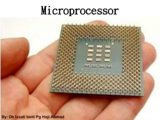
Microprocessor
450 likes | 653 Views
Microprocessor. Dr. Rabie A. Ramadan Al-Azhar University Lecture 3. Review. What are the four operations commonly performed by the MPU? Memory Read Reads instructions or data from the memory Memory Write Writes instructions and data into memory I/O Read

Microprocessor
E N D
Presentation Transcript
Microprocessor Dr. Rabie A. Ramadan Al-Azhar University Lecture 3
Review • What are the four operations commonly performed by the MPU? • Memory Read • Reads instructions or data from the memory • Memory Write • Writes instructions and data into memory • I/O Read • Accepts data from input devices • I/O Write • Writes data to output devices
Question • What is the function of address Bus ? • Holds memory or I/O addresses • How many memory locations can addressed by the MPU with 13 address lines ? • 213 • How many address lines are necessary to address two MB with 8-bit word size? • 21 lines
Question • Specify the number of Registers and Memory cells in a 128 X 4 memory chip? • 128 registers and 4 memory cells per register • How many bits are stored by a 256 X 4 memory chip? Can this chip specified as 128-byte memory? • 256*4 • No
Question • If the memory chip size is 1024 X 4 bits , how many chips are required to make 4K (4096) bytes of memory ? • two chips forms 1K memory • We need 8 chips
Question • Given the following Figure , define • How many words ? • How many bit per word? • How many address lines are used? • What is the name of the used bus? CPU Memory 1024 X 16 16 bit BUS
Question • State the steps required by the MPU to read or write from the memory?
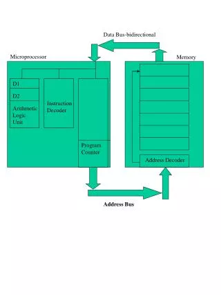
How the MPU Writes into the Memory? • MPU places the 16 bit address on the address bus • Memory interfacing circuits will decode address to specify the target register • MPU Places a byte on the data bus • MPU sends a control signal (Memory Write) to the memory to write
How the MPU reads from the Memory? • MPU places the 16 bit address on the address bus • Memory interfacing circuits will decode address to specify the target register • MPU sends a control signal (Memory Read) to the memory to enable the output buffer • The memory puts the data on the data bus and the processor will read it
Question • Define the following terms: • Byte addressing • Hit • Miss • SSI • VLSI • EBCDIC • ASCII • Compiler
Z80 Hardware and programming Model • 8-bit Microprocessor • 16- bit address lines • +5 V Power Supply • Housed in 40 pin dual in Line (DIP) – 2 sides • different versions of Z80 microprocessors such as Z80, Z80A, Z80B and Z80H • rated to operate at various frequencies ranging from 2.5MHz to 8MHz.
Signal Classification • All the signals can be classified into six groups. • address bus • data bus • control signals • external requests • request acknowledge and special signals • power and frequency signals
Address Bus • 16 tri-state signal lines, A15 – A0 • unidirectional and capable of addressing 64K (216) memory registers • used to send (or place) the addresses of memory registers and I/O devices. • Tri state (0 , 1 , high impedance (the output has no effect )
Data Bus • eight tri-state bidirectional lines D7 – D0 • used for data transfer. • data can flow in either direction-from the microprocessor to memory and I/Os or vice versa.
Control and Status Signals • Five individual output lines: • three can be classified as status signals indicating the nature of the operation being performed, • two as control signals to read from and write into memory or I/Os.
Control and Status Signals • Machine Cycle One: • Status line indicates that an opcode is being fetched from memory. • Also used in an interrupt operation to generate an interrupt acknowledge signal.
Control and Status Signals • Memory Request: • indicates that the address bus holds a valid address for a memory read or writes operation.
Control and Status Signals • I/O Request: • Active low tri-state line • Indicates that the low-order address bus (A7 – A0) holds a valid address for an I/O read or writes operation.
Control and Status Signals • - Read: • Indicates that the microprocessor is ready to read data from memory or an I/O device • Used in conjunction with for the Memory Read ( ) operation • Used in conjunction with for the I/O Read ( ) operation.
Control and Status Signals • – Write: • Indicates that the microprocessor has already placed a data byte on the data bus and is ready to write into memory or an I/O device • Should be used in conjunction with for the Memory Write ( ) operation • should be used in conjunction with for the I/O Write ( ) operation.
External Requests • Includes five different input signals to the microprocessor from external sources. • Used to interrupt an ongoing process and to request the microprocessor to do something else.
External Requests • – Reset: • used to reset the microprocessor. • Clears the program counter (PC), the interrupt register (I), and the memory refresh register (R). • Everything is in reset state –e.g. address bus and the data bus are in high impedance state
External Requests • – Interrupt Request: • initiated by an external I/O device to interrupt the microprocessor operation. • When the microprocessor accepts the interrupt request, it acknowledges by activating the signal • The signal is maskable, meaning it can be disabled through a software instruction.
External Requests • – Nonmaskable Interrupt • It cannot be disabled. It is activated by a negative edge-triggered signal from an external source. • Used primarily for implementing emergency procedures. • No Ack signal is generated
External Requests • – Bus Request: • Initiated by external I/O devices such as the DMA (Direct Memory Access) controller • An I/O device can send a low signal to request the use of the address bus, the data bus, and the control signals. • The external device can use the buses and when its operations are complete, it returns the control to the microprocessor.
External Requests • – Wait: • This signal is used when the response time of memory or I/O devices is slower than that of the Z80
Request Acknowledge and Special Signals • BusAcknowledge: • Initiated by the Z80 in response to the Bus Request signal. • Indicates to the requesting device that the address bus, the data bus, and the control signals have entered into the high impedance state and can be used by the requesting device.
Request Acknowledge and Special Signals • – Halt: • Indicates that the MPU has executed the HALT instruction.
Request Acknowledge and Special Signals • – Refresh: • Indicating that the address bus A6-A0 (low-order seven bits) holds a refresh address of dynamic memory; • Should be used in conjunction with to refresh memory contents.
Power and Frequency Signals • - Clock: • Used to connect a single phase frequency source. • The Z80 does not include a clock circuit on its chip
Power and Frequency Signals • +5V and GND: • These pins are for a power supply and ground reference; • The Z80 requires one +5V power source.
Z80 Programming Model • Accumulator and a flag register, • General-purpose register arrays, registers as memory pointers, and special-purpose registers.
General-Purpose Registers • Six programmable general-purpose registers named B, C, D, E, H, and L • 8-bit registers used for storing data during the program execution. • can be combined as register pairs – BC, DE, and HL – to perform 16-bit operations or to hold memory addresses
Accumulator • Part of the arithmetic logic unit (ALU) and is also identified as register A. • The result of an operation performed in the ALU is stored in the accumulator.
Flag Register • ALU includes six flip-flops that are set or reset according to data conditions after an ALU operation • D0 - D7 are the ALU status flag
Alternate Register Set • not directly available to the programmer • Used for internal operations
16-Bit Registers As memory Pointers • four 16-bit registers • used to hold memory addresses • Index Registers (IX and IY) • used to identify locations for data transfer. • Stack Pointer (SP) • point to the memory location called the stack. • The stack is a defined area of memory location in R/W memory
16-Bit Registers As memory Pointers • Program Counter (PC) • Used by MPU to sequence the execution of instructions • Special-Purpose Registers • two special-purpose registers that are generally absent in other 8-bit microprocessors • Described later
Machine Cycles and Bus Timings Next time