Download

1 / 18
180 likes | 283 Views
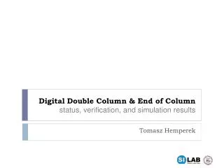
Sakari Tiuraniemi - CERN. End of Column Circuits. 40. 45. 5. 5. 5. 5. 9. 9. 9. 9. RX. RX. RX. RX. DLL 32-bit. address. address. address. address. TDC bank. TDC bank. TDC bank. TDC bank. PLL 320 MHz. registers. registers. registers. registers. serial. serial.

E N D
Sakari Tiuraniemi - CERN End of Column Circuits
40 45 5 5 5 5 9 9 9 9 RX RX RX RX DLL 32-bit address address address address TDC bank TDC bank TDC bank TDC bank PLL 320 MHz registers registers registers registers serial. serial. serial. serial. Ref CLK 40 MHz EOC Architecture
9 TDCs, each for a group of 5 non-adjacent pixels 32 to 5 bit encoders integrated with hit registers Instead of reading out all the 32 bits Avoid 32x2x9x40 parallel lines in the layout, decrease complexity of the following circuitry Encoders not used in the demonstrator 1 2 3 4 5 6 7 8 9 10 11 12 . . . 19 20 28 29 36 address TDC 1 32 to 5 bit TDC 2 32 to 5 bit TDC 8 32 to 5 bit TDC 9 32 to 5 bit 5 5 5 5 TDC per 5 pixels – EOC
TDC-bank Hit Registers: layout ready DLL- and TDC-bank Buffers: layout ready DLL VCDL: layout ready CP and PD layout under work Encoders: not designed 32 to 5 encoder Address encoder Post TDC circuitry: not designed PLL: not designed Design Status
32 delay elements 100ps delay each Phase detector Bang-bang detector only gives information of the sign of phase error Charge Pump Adjusts the delay by increasing/ decreasing control voltage by adding/removing charge in C Delay Locked Loop C
DLL – Charge Pump • Capacitance and current of Charge Pump affects • Accuracy of the delay (jitter) • Speed of the loop • Time to achieve lock • Response time for changes (in the clock phase, etc) • Need for further simulations to optimize capacitance size against speed • 1st order system - inherently stable loop • When higher order poles are at high frequencies
Icp = 1.72 µA C = 20 pF Kvcdl = 1.32 ns/V T = 1/fCLK = 3.2 ns Charge pump current is adjustable Possible to achieve fast locking time with higher current Increase accuracy after lock achieved with lower current Tlock = 1.329 µs Icp = 1.72 µA From VRFN = 600 mV (down to ~485.7 mV) DLL – Charge Pump
Jitter at the last delay element output Δτ = 13.713 ps With C = 20 pF Icp= 1.72 µA DLL – Jitter, Transient Analysis
DLL – Jitter, Transient Analysis • Jitter at the last delay element output • Δτ = 13.713ps • With • C = 20 pF • Icp= 1.72 µA • Delay of the last delay element • τ = 100.6 ps± 0.1283 ps • VRFN = 485.7mV ± 0.18 mV
Jitter at the last delay element output Δτ = 18.11 ps With C = 20 pF Icp= 1.72 µA DLL – Jitter, Transient Noise Analysis
DLL – Jitter, Transient Noise Analysis • Jitter at the last delay element output • Δτ = 18.11ps • With • C = 20 pF • Icp= 1.72 µA • Delay of the last delay element • τ = 100.5 ps± 0.1554 ps • VRFN = 493.4mV ± 0.18 mV
Status of Work - NEXT 1. Finish layout of DLL 2. Post-layout simulations with DLL and TDC 3. Start design work for PLL and post TDC circuits (shift registers and logic)