Download
1 / 39
390 likes | 397 Views
End OF Column Circuits – Design Review. Sakari Tiuraniemi. 40. 5. 5. 5. 5. 45. 9. 9. 9. 9. RX. RX. RX. RX. DLL 32-bit. address. Fine HR bank. address. Fine HR bank. address. Fine HR bank. address. Fine HR bank. Ref CLK 320 MHz. C-CNT 32-bit. Coarse HR bank.

E N D
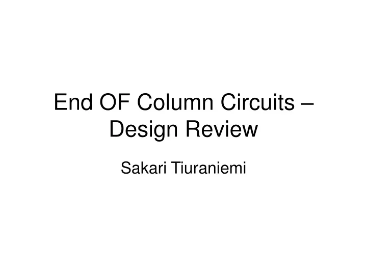
End OF Column Circuits –Design Review Sakari Tiuraniemi
40 5 5 5 5 45 9 9 9 9 RX RX RX RX DLL 32-bit address Fine HR bank address Fine HR bank address Fine HR bank address Fine HR bank Ref CLK 320 MHz C-CNT 32-bit Coarse HR bank Coarse HR bank Coarse HR bank Coarse HR bank registers registers registers registers serial. serial. serial. serial.
40 columns of 45 pixels Total of 1800 pixels Only analogue circuits in the pixel pre-amplifier, discriminator Differential current mode transmission of output pulse via transmission line 9 transmission lines shared with 5 pixels 5 transmission lines for group address (5 goups of 9 pixels) All noisy digital circuits in the periphery of the pixel array DLL, coarse count, time stamping and data processing and transmission (lvds) Each end of column consists of register banks 18 fine hit registers 36 coarse hit registers One DLL (and coarse counter) to drive 40 End of Column blocks Needs good buffering Pixel output converted into CMOS level pulses to trigger hit registers Trigger for both leading and trailing edge LVDS for off chip transmission End Of Column Architecture - overview
1 End OF Column- block will be implemented for the folded column (and 1 for the short column of 9 pixels) In addition one DLL+TDC w/ RX is implemented to test DLL EOC consists of RX cell (9+5 receivers) Fine HR bank (18) Coarse HR bank (18/36) Address HR bank (5) 32 cell DLL (320 MHz) 32-bit Coarse counter The immense amount of data is read out serially w/ LVDS One LVDS driver per TDC 9x5 pixel (folded column) demonstrator - EOC RX RX DLL 32-bit address Fine HR bank Ref CLK 320 MHz C-CNT 32-bit Coarse HR bank registers serial. 9 LVDS
DLL 32 delay cell voltage controlled delay line to provide fine time information for fine HR Delay of the delay line is adjusted (and ‘locked’) to match one reference clock cycle (3.125 ns) Delay of each cell is ~97.66 ps resulting in a 3.125 ns time span Coarse Counter (32 bits) Consists of two counters with opposite phases two provide a stable coarse time (at all times) for coarse HR Selection of counter output made according to fine time information Hit registers 32 cell registers build of D-type flip flops Each hit register is implemented with shift register to provide serial output as from the start To avoid readout lines filling the whole periphery of the chip Receiver Receiver cell gives a CMOS output with timing and pulse width information (see pres. of Pierre) Followed by a transition detection circuit to generate two signals: HIT_lead and HIT_trail used for triggering the corresponding HR End OF Column Circuits
t0 t1 tN-2 tN-1 τ0 τN-2 τ1 τN-1 VCDL Ref CLK UP VCTRL PD CP DOWN DLL CLK Delay Locked Loop - DLL • Delay locked loop • Voltage controllable delay line (VCDL) of 32 delay cells • Phase detector • Bang bang • Charge pump • Output buffers • Differential and • Single-ended
Christian’s DLL downscaled to ~100ps Only delay cell, buffers and its bias circuit needed to be redesigned Device size and bias current scaled down pmos loads 2 µm, nmos current source 2 µm, input pair nmos 4 µm Ibias = 86 µA, Vsupply = 1.2 V 103 µW per delay cell Differential Buffer: 625 µA Single-ended buffer: 69 µA 27.58 mW for 32 delay cells, phase detector and charge pump Delay τD ≈ 97.66 ps A differential output buffer is introduced to provide ‘lvds’ level signal to be distributed over the whole length of the chip (40 Fine HR banks (18 registers per bank)) The buffer is not needed in demonstrator, but is left in the design A single-ended buffer is to provide CMOS level signal to Phase Detector In front of each of the 40 fine HR banks there’s another single-ended buffer to provide CMOS level signal to hit registers data input Phase detector, charge pump and start up circuit identical to Christian’s Delay Locked Loop - DLL
Delay Element with buffers
Up left: DLL non-buffered differential output Up right: DLL buffered differential output Right: DLL buffered single-ended output (outputs of delay cells 15 and 16) DLL - simulations
VCTRL variation induced jitter at the last delay element output Δτ = 13.713 ps With C = 20 pF Icp= 1.72 µA Jitter at the last delay element output Δτ = 10 ps With C = 50 pF Icp= 1.72 µA DLL – Jitter, Transient Analysis
2 x 32-bit synchronous counter 180 degree phase difference to provide a steady output at all times Selection of coarse counter output to be organized to avoid reading output when changing state Using the fine time information Selection either on chip or off chip Coarse Counter
Ripple carry counter is too slow for a 32-bit counter @ 320 MHz Carry look-ahead scheme applied: Dividing the counter into 4-bit blocks Cout for the 4 bit block is provided by looking at the outputs and Cin Coarse Counter • Example 4-bit synchronous counter: • Instead of load, reset is applied to set the state of the counter to ‘0000’ through D0, D1, D2, D3 • Reset is latched with CLK
Time to Digital Converter • Tapped delay line • 32 cells, 97 ps • Two hit registers • One for leading and one for trailing edge • Shift registers together with hit registers are used to provide serial output data • One DLL is providing the fine time for each of the 40 end of column consisting • One EOC consists of 18 fine HR and 36 coarse HR • Coarse HR gets time from coarse counter • Only 1 EOC in the demonstrator Shift Register 1 trigger Hit Register 1 t0,t1,t3,…,tN-2,tN-1 DLL Ref CLK trigger Hit Register 2 Shift Register 2
Fine HR 32 D-flip flops Buffer stage driving clock input Differential to single-ended buffer stage driving data input Bank level Shift register implemented to side Coarse HR 2x32 D-flip flops Buffer stage driving clock input Single-ended buffer stage driving data input Bank level Shift register implemented to side Hit Registers
Receiver Bank consists of 9 + 5 receiver cells (Pierre) Each receiver is followed by a transition detection circuit which provides two signals: HIT_lead and HIT_trail The length of the pulse is provided by a delay line (current starved inverters) The two signals are used to trigger hit registers for fine and coarse time The HIT_trail is also used as a control signal to: block possible overlapping hits (by disabling the output buffer) set a flag for ‘ready to read the shift registers’ Transition detection: A B Start Stop τ Receiver
An additional delay of 260 ps is introduced due to the D-flip flop and the buffer stage Blocking following hits until HR is read is done by having the first buffer inverter disabled Each trigger signal drives 3 hit registers Additional buffer stage in each HR Trigger generation
RX PG Fine HR Bank Coarse HR Bank DLL Coarse CNT
Fine HR Bank Coarse HR Bank 300 µm VCDL 1 Coarse counters 2 Charge Pump Filter 770 µm
9 TDCs, each for a group of 5 non-adjacent pixels 32 to 5 bit encoders integrated with hit registers Instead of reading out all the 32 bits Avoid 32x2x9x40 parallel lines in the layout, decrease complexity of the following circuitry Encoders not used in the demonstrator 1 2 3 4 5 6 7 8 9 10 11 12 . . . 19 20 28 29 36 address TDC 1 32 to 5 bit TDC 2 32 to 5 bit TDC 8 32 to 5 bit TDC 9 32 to 5 bit 5 5 5 5 TDC per 5 pixels – EOC