Download
1 / 39
390 likes | 578 Views
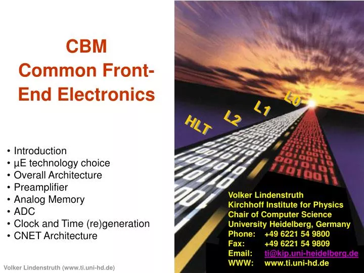
L0. L1. L2. HLT. CBM Common Front-End Electronics. Introduction µE technology choice Overall Architecture Preamplifier Analog Memory ADC Clock and Time (re)generation CNET Architecture. Volker Lindenstruth Kirchhoff Institute for Physics Chair of Computer Science

E N D
L0 L1 L2 HLT CBM Common Front-End Electronics • Introduction • µE technology choice • Overall Architecture • Preamplifier • Analog Memory • ADC • Clock and Time (re)generation • CNET Architecture Volker Lindenstruth Kirchhoff Institute for PhysicsChair of Computer Science University Heidelberg, Germany Phone: +49 6221 54 9800 Fax: +49 6221 54 9809 Email: ti@kip.uni-heidelberg.de WWW: www.ti.uni-hd.de
The CBM Experiment • Radiation hard Silicon (pixel/strip) Tracking System in a magnetic dipole field • Electron detectors: RICH & TRD & ECAL: pion suppression better 104 • Hadron identification: TOF-RPC • Measurement of photons, π0, η, and muons: electromagn. calorimeter (ECAL) • High speed data acquisition and trigger system
Key Challenges Remember: no trigger systen – FEE has to implement that on a per channel basis • Global coherent clock/time distribution ~1ns • Low-cost data readout • Hit detection/selection (CNET) next neighbor communication • Common front-end electronics • (very high rate) readout for vertex detector • Generic Preamplifiers – modular amplifiers??
Making Chips …. A. Marchioro (CERN)
TRAP3 reticle OASE-1 ATOLL TRAP UMC 180nm, 8“
Overall Electronics Requirements • Three Categories • Silicon Tracker • Radiation tolerance 60 MRAD • Time resolution <10 ns (we may have to accept pile-up) • Channel count 2M (ITS) ~1M (STS) • Channel area (25 µm)2 • Time of Flight System • Radiation tolerance ~100 kRAD • Time resolution 25 ps • Channel count 60k • Channel area (50 mm)2 • TRD, RICH, ECAL • Radiation tolerance ~100 kRAD • Time resolution <10 ns • Channel count (>600k, 120k, 23k) • Channel area [cm2] (1, 0.4, 10) • One solution ??? – maybe two or three ???
Common Front-End Electronics preFilter digital Filter Hit Finder Backend & Driver PreAmp ADC • Si Strip • Pad • GEM's • PMT • APD's Anti-AliasingFilter Sample rate: 10-100 MHz Dyn. range: 8...>12 bit 'Shaping' 1/t Tailcancellation Baselinerestorer Hit parameter estimators: Amplitude Time Clustering Buffering Link protocol Detector specific generic
Technology Considerations • Radiation Hardness • Not an issue for DSM – Vertex Detector may be an exception • Speed • Not a critical issue for CBM • Routing • Experience with existing designs show that 6 routing layers are typically sufficient • Power • Reduces for smaller process sizes, current does not • Cost • Factor 2 cost for MPW and Engineering run between 180 and 130 nm • Existing Expertise, IP • Huge amount of existing IP cells and analog designs with appropriate experience with the process available • Conclusion • Use UMC 180nm process as baseline process until critical issues require technology migration
. . . Over All Architecture to/from next neighbor hit detection • Hit Detector • Leading Edge • peak • … N Pre- Amplifier Blocks Programmable Finite State Machine DATA-out send Fast Readout DAC start Digital Pipeline Hit TDC TIMER stop Ain CLOCK we 1..N Event Buffers WE RE sample Digital Filters ADC • different combinations • sampling rate • resoluion • power ANALOG FIFO Analog Filter to/from next neighbor hit detection
The TAC Core • Digital delay chain • Distributed RC-Network • Voltage on Cout increases linear with time Various other approaches suggested also (DLL, ....)
Analog Memory Switched capacitor analog memory Data lifetime @ 10 Bits [# of samples] Switched current analog memory Temperature [deg C] David Muthers, Kaiserslautern
Common ADC David Muthers, Kaiserslautern
Common ADC David Muthers, Kaiserslautern
ADC Considerations • PreAmp for 12 bit resolution = 72 dB SNR and THD 72 dB loop gain + 34 dB closed loop gain = 106 dB @ fT= 40 MHz • 1 LSB = 245 µV 310 e @ Cfb = 200fF • Thermal noise of feedback R / C @ Cfb=200fF = 150 µV (kT/C) • Input referred noise of PreAmp is amplified by A = 1+ Cfb/ Cshunt = ~100 ( 40dB) 150 µV / 100 = 1.5 µV !!! (including pick up) • Differential input helps to reduce pick up of noise irradiation • PreAmp should be attached very close to detector PAD in order to reduce Cshunt • Pulse shaping by zero of PreAmp transfer function reduces required dynamic range and hence saves power • High order lowpass (Gm/C) filter is natural companion of AD-converter/digital chip • Jitter Constraints on digitization clock (@12-Bit, 40 MSPS, 20 MHz input): 12 ps for 0.3 LSB max. quantization error
2.5 GBit/sec SERDES @ UMC 180nm • TX works (c.f. eye pattern) • Clock generation 13.7 ps jitter • Serializer power (sim) 180 mW • RX being tested Sitt Tontisirin, Kaiserslautern
transimpedance Amplifier & limiting amplifier control & status registers control & debug interface parallel interface output parallel interface input clock & data recovery pre- equalization laser driver with PhDet 8B/10B decoder 8B/10B encoder CML Output CML input deserilaizer laser driver serilaizer to VCSEL on-chip to VCSEL off-chip to optical transceiver from optical transceiver from PIN diode SerDes / Clock Recovery
BuTiS – Bunchphase-Timing-System A broadband propagation delay stabilization scheme Optical Receiver (Detector) Echoed stream propagation delay 3-Port Circulator Pilot Delay Control Variable Optical Delay Laser Diode/Modulator Optical Receiver (Detector) MPX Stream with Pilot Signal Forward stream propagation delay The optical delay is by nature broadband, covering a whole waveband (1310 or 1550nm)
BuTis Summary • Use of broadband optical RF-links and single mode fibers are • mandatory, most components can be purchased from stock • The fiber properties need careful attention to reach 100ps@1km • A „BuTiS“- like system will surely be needed for FAIR accelerators • BuTiS has „campus-wide“ capabilities for realtime synchronisation and timing • At present conceptual design stage, system modifications can be realized without costly modifications • It can be build with moderate costs at the beginning, and later extended to a very sophisticated topology
Clock and Timing distribution • Fiber optics have become a commodity • High speed readout serial anyway • Use of glas as media simplifies grounding • Half- and full diplex almost same price • DCS functionality requires negligible fraction of downlink • Use available uplink and fraction of downlink for DCS network (and others) • Multi gigabit deserializers require very stable, low jitter clock recovery • Why not use serial infrastructure also for clock and time distribution • advanced optical serializer/deserializer
Ternary CAM Cell • Save ~20% of area by optimized design: • store 1/0 for a 1 • store 0/1 for a 0 • store 0/0 for don’t care (cell does not participate in match calculation) • Cell size is 10.82 µm x 2.69 µm write match power down
Power Regulators Issues • FEE is operated in magnetic and ionizing areas • FEE power requirements continue to move to lower voltages <1V and high currents (Amperes) • Copper significant cost and material factor • Distributing LV from outside the detector requires traveling long distances • Regulators required on detector close to electronics • LV power distribution in TRD requires about the same power as entire electronics (part goes in to voltage drop in copper and part into regulators on detector) • There are no good low drop, high current voltage regulators
Power Regulators Requirements • Step Down regulator from moderately filtered external DC supply (e.g. 40V) • Tolerance against radiation (not radiation hard) • Tolerance against magnetic fields • Feasibility of a transformer with compensation coils for magnetic field • Transformator saturation can be measured and compensated for automatically • Very low noise (output and generated in environment) • Small outline • High efficiency • Run at high frequency (100 MHz?) for better filtering later and for staying away from most relevant analog frequency domains • Implement digital sequencers to generate externally triggered power profiles (proactive regulation) • Small sequencer chip plus external power transistor • Lets start this project as Ph.D. thesis and not miss the boat again.
to/from next neighbor hit detection • Hit Detector • Leading Edge • peak • … N Pre- Amplifier Blocks Programmable Finite State Machine DATA-out send Fast Readout DAC start Digital Pipeline Hit TDC TIMER stop Ain CLOCK we 1..N Event Buffers WE RE sample Digital Filters ADC • different combinations • sampling rate • resoluion • power ANALOG FIFO Analog Filter . . . to/from next neighbor hit detection Over All Architecture Need global, synchronous time reference
Summary • CBM defines a new set of challenges in front-end electronics • Many key issues identified, many left for additional work • One baseline technology, common interfaces and tooling to save cost and effort Note: slides were compiled from various sources and may not allways cite authors correctly
Open Questions • Open questions concerning both, TAC and DLL solution • TDC resolution required? • Single / double hit resolution? • Double hit only flagged? • Integration Level (Geometry)? • Event rate to cope with (100 kHz)? • Discriminator specs (time over threshold)? • min. and max. signal length • double hit resolution • Temperature? • Radiationhardness? • Interfaces? • Discriminators, clock distribution, DAQ
New chip TC3 with lager devices, PMOS pair,… • All MOS wider, but still minimum length for speed! This is bad for matching… • Detail of VCO (Ringoscillator): current sources under wide power busses VCO inverter ‘small’ inverter interconnect between VCO stages(in light blue…) loads under wide power busses
Summary • Differential logic with diode-clamp load works (also at high speed). (This may not be the best solution!) • Timer with ring oscillator, buffers, latches,… works • PLL locks • Matching is a big issue. • Observed mismatch cannot be reproduced by Monte Carlo Simulations. • Consequences: Submit matching test structures, or try out sizing… • Time bin width of 150 ps achieved at 100µA in 0.35µm • This leads to a single channel resolution (after correction of bin width) of s = 55ps, including mismatch • Expected improvement by going to 0.18µm is at least a factor of 2 (at same current, large devices) • Another factor of two by increasing current. • Can probably use a bit shorter MOS than in simulation.. • In total, s = 15ps seams possible in 0.18µm with no further tricks. • Most of the presented work has been done by Michael Ritzert
Status & Plans • Layouts of crucial (dense) blocks is done: CAM cells, Flipflops, row decoder (F. Giesen’s Diploma Thesis) • Most simulations (typical parameters) are done.Speed is >500MHz for a CAM with 512 rows (parasitics of busses included) • We plan to submit an 512 x 18 bit block (testing maximum speed needs full size!).Layout area of this core will be 0.3mm x 1.4mm • Testing will be done by setting all input bits & reading all output bits with shift registers.Timing will be generated by several external fast strobe signals.This stuff will be synthesized (with help from Rechnerarchitektur) • We are confident to be ready until April 24. : done : missing
Submission Plans • Boundary condition 5x5 mm2 ADC Test structures (Muthers) PLL structures (Tontisirin) Full Custom CAM Test Structures DAC Ring Oscillator Peter Fischer • Boundary condition 1.5x1.5 mm2 FC CAM Fischer TsT PeFi
Summary • First CBM FEE Meeting • Technology Baseline Choice UMC 180nm • Many existing building blocks and developments • Several key issues/items identified: • Preamplifier • ADC • Clock Recovery (good enough for ToF?) • Serializer • Integration with BuTis • Two MPW submissions foreseeable • April 5x5 mm2 some space left • June MiniASIC 1.5x1.5 mm2 • We need a FEE recess soon to discuss many of the outstanding preamplifier issues