Download
1 / 29
300 likes | 316 Views
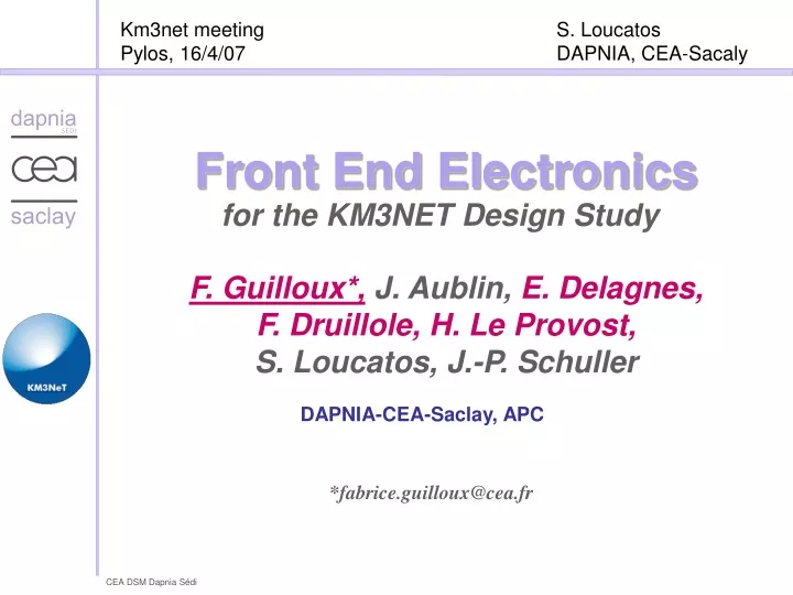
Km3net meeting Pylos, 16/4/07. S. Loucatos DAPNIA, CEA-Sacaly. Front End Electronics. for the KM3NET Design Study. F. Guilloux*, J. Aublin, E. Delagnes, F. Druillole, H. Le Provost, S. Loucatos, J.-P. Schuller. DAPNIA-CEA-Saclay, APC. *fabrice.guilloux@cea.fr.

E N D
Km3net meeting Pylos, 16/4/07 S. Loucatos DAPNIA, CEA-Sacaly Front End Electronics for the KM3NET Design Study F. Guilloux*, J. Aublin, E. Delagnes, F. Druillole, H. Le Provost, S. Loucatos, J.-P. Schuller DAPNIA-CEA-Saclay, APC *fabrice.guilloux@cea.fr
Antares Front End (VFE) sum up • First Level Functionalities: • Discriminate signals coming from the PMT. • Measure their arrival time (0.5 ns rms precision). • Measure their charge. • Bufferize and Derandomize the event flow. • 2nd Level Functionalities: • Rate Monitor + rate alarm. • Filter by L1 and L2 (historical reason). • Test Led generator … • All this for a reasonable power consumption and a low cost. • Antares readout electronics Ethernet Network Optical Module Analog Ring Sampler ARS Board DAQ Board • VFE requirements • Convert charge & time in digital data. • Format the events & serialize them toward the DAQ board. • Oscilloscope mode.
Antares Front End (VFE) sum up • Solutions developed in the Analog Ring Sampler ASIC WaveForm : 128 memory cells ADC SPE Charge Integrator + Time to Voltage Converter Pulse Shape Discriminator
ARS feedback - • Strength and weakness + • Too many functionalities and parameters hard to test • Asic mainly asynchronous hard to simulate • Two ASICs per OM (to minimize dead time) Should be done by one • Time precision : 500ps rms • Measure Charge of SPE without a delay added to signal path • Waveform : • Fast sampling : 640MHz (up to 1GHz) • 128 memories depth for 3 amplitudes - The AMS 0.8µm is not available any more The ARS reaches expected performances but it is too complicated : the architecture could be improved to make it simpler
KM3NET conservative solution: • Reuse of Antares development, updated in order to fit to KM3NET specific requirements: • OM ASIC DAQ Ethernet network • “Input” specifications (Conceptual Design 1 & 2 from WP4) • PMT electrical signal characteristics : 10’’ from Antares • Amplitude : typically a few tens of mV per PE • SPE Pulse time: all the signal is included in a window of 20ns • Reference clock frequency : few tens of MHz • Slow control protocol • Physic requirements • Measure charge with DQ/Q < 10% • Measure arrival times with 0.5ns rms precision • Input dynamic range~ up to 100 pe • Input rate : up to 200kHz in average (SPE), max. 500kHz during 1s • Discriminate multi-muon bundles Antares updated requirements Km3Net requirements • Scale effects Consumption, Design simplifications • Cost reduction Design Optimizations
New VFE Asic: Submarine Cherenkov rAdiated Light Electronic (SCALE) SPE memory SPE memory SPE memory SPE memory SPE memory SPE memory SPE memory SPE memory ADC 8 Ch Dg 8 bits DLL DLL DLL DLL DLL DLL DLL DLL L0 Infos PSD Anode L0 accepted L0, WF WF valid … Switch Array Capacitors 16*32 = 512 ADC 32 Ch Dg 8 bits Delay Locked Loop
Scale : key points • The memory Cell • Ring memories keep the past of the signal No need of external delay line • Fine Time and charge are extracted from the same unit Simplification • Fine Time is extracted from a Delay Locked Loop No ADC needed to convert time information : it is naturally digital Easy to calibrate : possible to reach ns precision from a 20MHz input reference clock with few spread (feedback loop) Clock DLL Trigger Fine Time (~6 bits) Signal IN Signal OUT Switch Capacitors Array • Multi-channels Wilkinson ADC • 8 bits resolution, ~ 5MHz conversion frequency • Architecture simplification • One Asic up to 500kHz (SPE) Queuing theory : probably 2 banks of 4 memories
High level language Simulations • Simulations scheme Shape discriminator Bias ADC Digital Control 8 memories Digital Fifo Digital Mux
High level Simulation Results • Signal filtering • Dynamic range ~ 100 pe • Integrated charge error < 10% • Time resolution < 0.5ns rms • Digital output • Charge : 10 bits • Fine Time : 6 bits • TimeStamp : 24 bits Transistor level simulations are in progress
Other solution under study: Multi-threshold discriminator • Discrimination strategy • Arrival time and TOT is given by several discriminators. Input Threshold1 Threshold2 • SPE and others signals are treated the same way : no need of waveform • The electronics is simpler : minimal analog circuitry • Is it possible to find the charge with enough accuracy knowing only the TOTs ?
Experimental setup ANTARES Optical Module LED triggered by generator pulses Acquisition by digital oscilloscope (2.5 GHz)
p.e. study Acquisition of 1000 pulses without flasher with the LED Trigger on p.e. background Charge integration: Q = Vi x ti. ,or better:Simpson integral Average track estimation
Using the LED Runs with several LED intensities
Signal shape Fit with sum of 4 gaussians or gamma distribution : Fit on the average low amplitude signal then fit 1 parameter only (normalization).
Relation ToT-Charge • Threshold values tested: • Th= 1/3 PE • Th = 2/3 PE • Th = 1.5 PE • Th = 5 PE • Th = 10 PE • Th= 20 PE • Th = 40 PE Fit: ToT = A + B* Ln( Charge / Charge 1p.e.) Constants A et B to be determined for each threshold value
Charge and time reconstruction • Time is given by crossingof the first threshold. “walk” effect, need of the amplitude or charge for correction. • Charge reconstruction: 3 methods • Fit by a pulse form • TOT ~ Ln (Q) • Geometrical approximation
Data quality • Dispersionof time of the LED emission • Oscilloscope window reduced in amplitude Quantification noise >> electronic noise
Fit method • Hypothesis : If all the photons are perfectly synchronous, the curve of the output of PMT is homothetic to the SPE curve. • Méthod : • We fit the average curve of SPE by a parametrised curve (A0,T0) • We fit the pairs of points of threshold crossings by this parametrised curve • Conclusions: • Good charge reconstruction in the entire range (~ +/- 10% RMS) • Sensitive to the LED dispersion de la LED (but systematic deviation correctible) • Very sensitive to the number of thresholds
Expected time dispersion Photon arrival times in water (incl. Antares electronics DT) The dispersionof the LED emission has some similarity with Cerenkov data
TOT method • Hypothesis : • TOT ~ Ln (Q) • Méthod : • For each threshold we find points (A,B) such that : TOT = A + B * Ln(Q) • We use then the inverse function • Conclusions : • Sensitive to the fit for (A, B) • Sensitive to double non simultaneous pulses! • After strong filtering and using the correction, then approach 10%
Amplitude Seuil 3 Seuil 2 TOT1 Seuil 1 Temps Geometrical method • Hypothesis : • The simplest method to compute the charge : the area under the curve • Method : • Linear interpolation between points • Interpolation TOT1 = A+B*Ln(Q) for the last threshold • Conclusions: • Very efficient for high charges • Sensitive to the start and exponential decrease at small charge (few points)
Time reconstruction + walk correction • Hypothesis : • Why go through the charge in order to correct time ? • Méthod : • For each threshold, we find points (A,B) such that : Tpic = A*TOT² + B*TOT+C+Tinit
Time reconstruction + walk correction • Resuts : • With 8 thresholds : error on Tpic ~ 300ps RMS • With 3 thresholds : error on Tpic ~ 800ps (sigma), even with our digitisation error. But: double pulse recognition difficult with 3 thresholds • Conclusion : • With TOT exact computation (error of 800ps) of arrival time • With thresholds, approximation of number of photons
Solution for TOT • Schémas 1 : Analogue Digital FPGA • Time coding • Data compression • Zero suppression • Charge and Time Simulation Test on Virtex V 500MHz 1ns 1ns + Simplicity : few components • Communication Discri – FPGA high frequency • Time precision : 1ns Fsampl≥1 GHz
Solution for TOT • Schémas 2 : Analogue Digital Clock FPGA n • Time coding • Data compression … … … n Data Discri. Sampling Data in parallel + Synchronous + Communication Discri – FPGA medium frequency • Volume of simultaneous data …
Discriminate signals coming from the PMT. • Measure their time (~ 0.5 ns rms precision). • Measure their charge. • Bufferize and Derandomize the event flow. • Convert charge & time in digital data. • Format the events & serialize them toward the DAQ board. • An Oscilloscope mode (Wave Form) • Rate Monitor + rate alarm. • Test Led generator. • … Amplitude T0 + few ns T0 Charge WaveForm Threshold T0 T0 + T1 Time VFE principle • Limited functionalities • Discrimination principle • Electrical Shape from PMT, in case of single photon, is known : Only arrival time (T0) and charge is needed. • In order to recognize patterns from multi-muon bundles, TOT larger than T0+T1 is treated as a Waveform
Résumé : Q > 10 PE 10 > Q > 2 2 > Q Amplitude Amplitude Amplitude Temps Temps Temps • Fit ne voit pas le 2e pulse • TOT surestime ou sous-estime la charge • Géo. bonne approximation • Fit et TOT: bonne approximation si pas de 2e pulse sous le 1er seuil • Géo. : pas d’interpolation possible • Bonne approximation de la charge, quelque soit la méthode.
Future developments • Complete schematic simulations • Scale Prototype : include in a new PMT readout scheme DAQ Board ARS Board • Board number reduction • Component number reduction System On Chip Objectives : • VFE • Antares compatibility • Tests in laboratory • OM integration (in the sphere) • Test in situ SoC VFE VFE PMT control • TOT option under study