Download
1 / 10
100 likes | 178 Views
Clock and Control Status. Matt Warren, on behalf of Martin Postranecky. Introduction. C&C fans-out machine clock and fast signals to 8x LDA (or DIF or ODR) Uses same HDMI cables and pinout as LDA-DIF. Plus more. Multiple types of signal input

E N D
Clock and Control Status Matt Warren, on behalf of Martin Postranecky
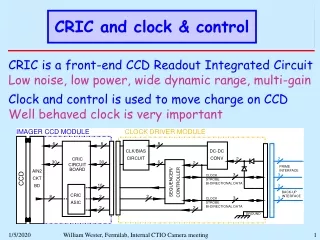
Introduction • C&C fans-out machine clock and fast signals to 8x LDA (or DIF or ODR) • Uses same HDMI cables and pinout as LDA-DIF. • Plus more. • Multiple types of signal input • Provision for async scintillator type signals (Fast Trig) • Also capable of aggregating and generating Busy feedback • Possible links to a controller and Run-Control ODR ODR DIF DIF Clocks C&C LDA Fast Trig Control LDA Busy x8 Run-Control LDA Martin Postranecky/Matt Warren - C&C Status
Overview • Hardware fan-out and fan-in • Standalone(external control optional) • Configured by jumpers • Local clock oscillator • Good signal integrity/safety • Clocks on dedicated lines, with PLL • Auto failover to local clock • Fast trigger on dedicated lines • Flexible • Multiple types if signal inputs and outputs for versatility • Jumper configurable signal loops for off-board signal control via header if needed Planned to keep it as simple as possible: CLOCK MPX + PLL XTAL FAST TRIG CONTROLS Jumper config BUSY PCB Header Simple! Not really. AND we could easily add …. Martin Postranecky/Matt Warren - C&C Status
C&C Logic and Interfaces Signal Inputs: • Clocks • 1x LVDS (SMA), 1x LVTTL (Lemo), 1x NIM (Lemo) • Fast Trigger • LVDS (SMA) • Controls (e.g. normal trigger) • 4x LVDS (SMA) • 4x NIM (Lemo) • Busy • 8x (HDMI) As the design matures many ‘little’ extras add up to a lot. The design now comprises: • CPLD (XCR3128XL-7) replacing many jumpers and switch logic • RS232 interface as a means of control • Many more buffers, 0Ω resistors and solder links for better signal integrity, isolation and configuration Signal Outputs: • 8x HDMI with LVDS Clock, Fast Trigger and Control • Clocks • 2x LVTTL on Lemo • 2x NIM on Lemo • 8x LVDS on SMA • Busy • LVDS on SMA • NIM on Lemo • OC-TTL on Lemo * Need to finalise RJ45 (and any other) interface to TLU (and others?) Martin Postranecky/Matt Warren - C&C Status
Overview Schematic Note: Clock and Fast-Trig handled by dedicated hardware, not CPLD. CLOCK AUTO/ XTAL SW LVDS on SMA LVTTL on Lemo 8x LVDS on HDMI NIM on Lemo MPX +PLL 8x LVDS on SMA 2x LVTTL on Lemo 2x NIM on Lemo ~ 50 MHz X-TAL FAST TRIG SW LVDS on SMA 8x LVDS on HDMI CONTROLS CPLD (Xilinx Coolrunner XCR3128XL-7) 4x LVDS on SMA 4x NIM on Lemo 4x 4 SW-2 5->1 4 8x LVDS on HDMI BUSY LVDS on SMA 1 SW-3 2->1 8x LVDS on HDMI NIM on Lemo 4 o/c TTL on Lemo RS232 PCB Header Martin Postranecky/Matt Warren - C&C Status
Some Hardware Details • Clock: • PLL/MUX - ICS581-02 • +/-150 ps jitter • 45min/55max Duty Cycle • Failover if external clock missing for 3 cycles. • Local Osc. 100 MHz/2 = 50% duty-cycle 50MHz • CPLD: Xilinx CoolRunner XPLA3 XCR3128XL-7 • 3.3V, low power • 128 macrocells with 3,000 usable gates • 5.5ns pin-to-pin logic delays • Extra IO via IDC header. • Single PCB with connectors at the edge (big!) • Separate PSU Martin Postranecky/Matt Warren - C&C Status
Status/Schedule • RAL doing schematics/layout and managing manufacture. • Were delays at RAL due to workload. • We have a complete design on paper. • Schematic entry now. • Layout mid-June (2 weeks) • Manufacture July/Aug Martin Postranecky/Matt Warren - C&C Status
The End. Backup slides follow … Martin Postranecky/Matt Warren - C&C Status
HDMI Pinout (same as LDA->DIF) Maurice Goodrick and Bart Hommels, University of Cambridge Martin Postranecky/Matt Warren - C&C Status
CALICE C&C MODULE - Connector List : ==================================== MP-UCL, 22 May 2008 8x HDMI CONNECTORS ------------------ pair 1 ( 1, 3, 2) => LVDS clock OUTPUT pair 2 ( 4, 6, 5) => LVDS data/prompt/trigger OUTPUT pair 3 ( 7, 9, 8) <= LVDS data/busy/feedback INPUT pair 4 (10,12,11) <= LVDS spare INPUT pair 5 (15,16,na) => LVDS async/fast-trigger OUTPUT OTHER OUTPUTS ------------- 8x (SMAx2) => 8x LVDS clock 2x LEMO => 2x LVTTL clock 2x LEMO => 2x NIM/TTL clock 1x (SMAx2) => 1x LVDS data/busy/feedback 1x LEMO => 1x o/c TTL data/busy/feedback 1x LEMO => 1x NIM/TTL data/busy/feedback OTHER INPUTS ------------ 1x (SMAx2) <= 1x LVDS clock 1x LEMO <= 1x LVTTL clock 1x LEMO <= 1x NIM/TTL clock 4x (SMXx2) <= 4x LVDS data/prompt/trigger 4x LEMO <= 4x NIM data/prompt/trigger 1x (SMAx2) <= 1x LVDS async/fast-trigger 8x (SMAx2) <= 8x LVDS data/busy/feedback INPUTS/OUTPUTS to a PC : ----------------------- 1x 2x26 0.1" Header = Inputs/outputs to a PC 1x 50-pin IDC = Inputs/outputs to a PC PLUS ---- 1x D-9 or PJ45 = RS232 interface 1x Molex 2x7pin 2mm Header = JTAG Interface 1x Molex 9-pin 0.1" Header = JTAG Interface 1x Vcc/+3V3/-5V2/GND in “Raw” Connector List Martin Postranecky/Matt Warren - C&C Status