Download

1 / 58
670 likes | 1.31k Views
8-Bit Gray Code Converter. By Martin Serena, Dang Ly, Khoa Ly. Overview. Gray Code Background Delegated Duties Method of Design Target Specifications Simulation Results Block Diagram Schematics, Symbols, Layouts, and Simulations Design References Conclusion. Gray Code Background.

E N D
8-Bit Gray Code Converter By Martin Serena, Dang Ly, Khoa Ly
Overview • Gray Code Background • Delegated Duties • Method of Design • Target Specifications • Simulation Results • Block Diagram • Schematics, Symbols, Layouts, and Simulations • Design References • Conclusion
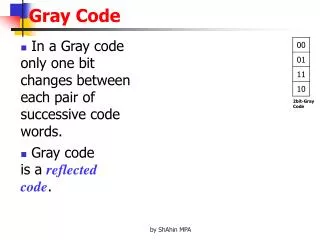
Gray Code Background • Conversion works in both directions • Binary Gray , Gray Binary • One bit changes from number to number • Not arithmetic • Not weighted (e.g. 222120) • Limits the amount of error that can occur when several bits change between numbers • No limit to number of converted bits
Binary to Gray Code Conversion 1 + 1 + 0 + 0 (BC) • MSB does not change as a result of conversion • Start with MSB of binary number and add it to neighboring binary bit to get the next Gray code bit • Repeat for subsequent Gray coded bits 1 0 1 0 (GC)
Gray to Binary Code Conversion 1 0 1 0 (GC) + + + • MSB does not change as a result of conversion • Start with MSB of binary number and add it to the second MSB of the Gray code to get the next binary bit • Repeat for subsequent binary coded bits 1 1 0 0 (BC)
Delegated Duties • Martin – Binary to Gray Conversion, Gray to Binary Conversion (XOR gates) • Dang – Binary/Gray Output Selection (MUXs) • Khoa – Binary Code Counter, Parallel-to-Parallel Shift Register (D flip-flops)
Method of Design • Decided on an initial load capacitance (Cin) • Partitioned the circuit into different propagation delay times according to gate/device requirements, and divided propagation delay times amongst the individual gates and devices • Created the symbol and layout for out each type of gate (XOR, MUX, NAND) • Connected gate symbols to create device symbols • Connected gate layouts to create device layouts • Connected device symbols to create circuit schematics, and connected device layouts to create circuit layouts
Target Specifications • Conversion: • Binary Code to Gray Code • Gray Code to Binary Code • Propagation delay times: • XOR (each): 0.4 nS • MUX (each): 0.3 nS • D flip-flop (each): 0.63 nS (worst-case fall time) • Technology specs (size): • Minimum Channel Width = 1.5 m • Minimum Channel Length = 0.6 m • Power < ¼ Watt • Clock Speed = 200 MHz • Total area as small as possible
Simulation Results • Successfully converts binary and Gray codes • Propagation Delay • XOR (each): 0.338 nS (worst-case) • MUX (each): 0.35 nS (worst-case) • D flip-flop (each): 1.14 nS (worst-case fall time) • Technology specs (size) • Transistor Lengths: 0.6 m • XOR: Wp = 3.9 m Wn = 3.75 m • MUX: Wp = 6 m Wn = 3 m • D Flip-Flop: Wp = 18 m Wn = 10 m
Simulation Results • Power (using the power meter) • 39.94 mW • Clock Speed • 200 MHz • Total Area • Gray code converter: 6.03E-4 cm2 • Counter: 10.2E-4 cm2