Download
1 / 52
520 likes | 653 Views
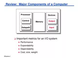
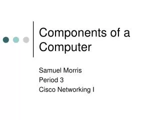
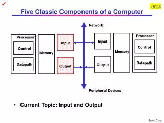
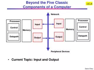
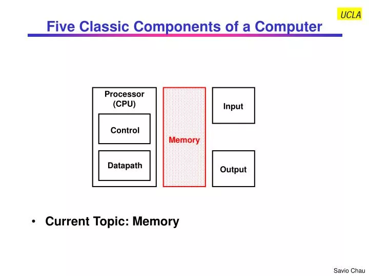
Five Classic Components of a Computer. Current Topic: Memory. Processor (CPU). Input. Control. Memory. Datapath. Output. What You Will Learn In This Set of Lectures. Memory Hierarchy Memory Technologies Cache Memory Design Virtual Memory. Memory Hierarchy.

E N D
Five Classic Components of a Computer • Current Topic: Memory Processor (CPU) Input Control Memory Datapath Output
What You Will Learn In This Set of Lectures • Memory Hierarchy • Memory Technologies • Cache Memory Design • Virtual Memory
Memory Hierarchy • Memory is always a performance bottleneck in any computer • Observations: • Technology for large memories (DRAM) are slow but inexpensive • Technology for small memories (SRAM) are fast but higher cost • Goal: • Present the user with a large memory at the lowest cost while providing access at a speed comparable to the fastest technology • Technique: • User a hierarchy of memory technologies Memory Hierarchy Fast Memory (small) Large Memory (slow)
Registers Cache Memory Disk Tape Typical Memory Hierarchy Performance: CPU Registers: in 100’s of Bytes <10’s of ns Cache: in K Bytes 10-100 ns $0.01 - 0.001/bit Main Memory: in M Bytes 100ns - 1us $0.01 - 0.001/bit Disk: in G Bytes ms 10-3 - 10-4 cents/bit Tape : infinite capacity sec-min 10-6 cents/bit
An Expanded View of the Memory Hierarchy Memory Secondary Storage Disk Memory Main Memory DRAM Memory Level 2 Cache SRAM Memory Level 1 Cache Memory registers Topics of this lecture set Topics of next lecture set
4 Do RA Instruction Memory WA Di I-Cache D-Cache L2 Cache Memory L2 Cache Mass Storage Memory Hierarchy and Data Path ExtOp ALUSrc ALUOp RegDst MemWr Branch MemtoReg RegWr Control Signals Control Signals Control Signals Main Control 4 PC+4 Adder Inst Mem
Charge Coupled Devices (CCD) Basic CCD Cell N-type Buried Channel Channel Stops Gate Gate Oxide Field Oxide Channel Stop Signal Charges Polysilicon Gates P-type Substrate Depletion Region Data Movement in CCD Memory for Reading/Writing 1-Pixel
Floating Gate Technology for EEPROM and Flash Memories • Data represented by electrons stored in the floating gate • Data sensed by the shift of threshold voltage of the MOSFET • ~104 electrons to represent 1 bit
Programming Floating Gates Devices Write a bit by electron injection Erase a bit by electron tunneling
Select = 1 P1 P2 Off On On On On Off N1 N2 bit = 1 bit = 0 SRAM versus DRAM • Physical Differences: • Data Retention • DRAM Requires Refreshing of Internal Storage Capacitors • SRAM Does Not Need Refreshing • Density • DRAM: Higher Density Than SRAM • SRAM: Faster Access Time Than DRAM • Cost • DRAM: Lower Cost per Bit Than SRAM SRAM Cell DRAM Cell Row Select (Address) Bit (Data) These differences have major impacts on their applications in the memory hierarchy
Wr Driver & Precharger Wr Driver & Precharger Wr Driver & Precharger Wr Driver & Precharger - + - + - + - + - + - + - + - + Sense Amp Sense Amp Sense Amp Sense Amp SRAM Organizations WrEn Precharge A0 Word 0 SRAM Cell SRAM Cell SRAM Cell SRAM Cell A1 A2 Word 1 Address Decoder SRAM Cell SRAM Cell SRAM Cell SRAM Cell A3 : : : : Word 15 SRAM Cell SRAM Cell SRAM Cell SRAM Cell Dout 3 Dout 2 Dout 1 Dout 0
DRAM Organization bit (data) lines Each intersection represents a 1-T DRAM Cell RAM Cell Array Row Decoder word (row) select Column Address Column Selector & I/O Circuits row address • Conventional DRAM Designs Latch Row and Column Addresses Separately with row address strobe (RAS) and Column address strobe (CAS) signals • Row and Column Address Together Select 1 bit at a time data
DRAM Technology • Conventional DRAM: • Two dimensional organization, need Column Address Stroke (CAS) and Row Address Stroke (RAS) for each access • Fast Page Mode DRAM: • Provide a DRAM row address first and then access any series of column addresses within the specified row • Extended- Data-Out (EDO) DRAM: • The specified Row/Line of Data is Saved to a Register • Easy Access to Localized Blocks of Data (within a row) • Synchronous DRAM: • Clocked • Random Access at Rates on the Order of 100 Mhz • Cached DRAM: • DRAM Chips with Built- In Small SRAM Cache • RAMBUS DRAM • Bandwidth on the Order of 600 MBytes per Second When Transferring Large Blocks of Data
1st M-bit Access 2nd M-bit 3rd M-bit 4th M-bit RAS_L CAS_L A Row Address Col Address Col Address Col Address Col Address Fast Page Mode Operation Column Address N cols • Fast Page Mode DRAM • N x M “SRAM” to save a row • After a row is read into the register • Only CAS is needed to access other M-bit blocks on that row • RAS_L remains asserted while CAS_L is toggled Row Address DRAM N rows N x M “SRAM” M bits M-bit Output
Why Memory Hierarchy Works? • The Principle of Locality: • Program Accesses a Relatively Small Portion of the Address Space at Any Instant of Time. Example: 90% of Time in 10% of the Code • Put All Data in Large Slow Memory and Put the Portion of Address Space Being Accessed into the Small Fast Memory. • Two Different Types of Locality: • Temporal Locality (Locality in Time): If an Item is Referenced, It will Tend to be Referenced Again Soon • Spatial Locality (Locality in Space): If an Item is Referenced, Items Whose Addresses are Close by Tend to be Referenced Soon.
Lower Level Memory Upper Level Memory To Processor Blk X From Processor Blk Y Memory Hierarchy: Principles of Operation • At Any Given Time, Data is Copied Between only 2 Adjacent Levels: • Upper Level (Cache): The One Closer to the Processor • Smaller, Faster, and Uses More Expensive Technology • Lower Level (Memory): The One Further Away From the Processor • Bigger, Slower, and Uses Less Expensive Technology • Block: • The Minimum Unit of Information that can either be present or not present in the two level hierarchy
Factors Affecting Effectiveness of Memory Hierarchy • Hit: Data Appears in Some Blocks in the Upper Level • Hit Rate: The Fraction of Memory Accesses Found in the Upper Level • Hit Time: Time to Access the Upper Level Which Consists of (( RAM Access Time) + (Time to Determine Hit/ Miss)) • Miss: Data Needs to be Retrieved From a Block at a Lower Level (Block Y) • Miss Rate = 1 - (Hit Rate) • Miss Penalty: The Additional Time needed to Retrieve the Block from a Lower Level Memory After a Miss has Occurred • In order to have effective memory heirarchy: • Hit Rate >> Miss Rate • Hit Time << Miss Penalty
Analysis of Memory Hierarchy Performance General Idea • Average Memory Access Time = Upper level hit rate Upper level hit time + Upper level miss rate Miss penalty • Example, let: • h = Hit rate: the percentage of memory references that are found in upper level • 1- h = Miss Rate • tm = the Hit Time of the Main Memory • tc = the Hit Time of the Cache Memory • Then, Average Memory Access Time = h tc + (1- h)(tc + tm) = tc + (1- h) tm Note: This example assumes cache has to be looked up to determine if miss has occurred. The time to look up cache is also equal to tc. • This formula can be applied recursively to multiple levels. Let: Let: The subscript Ln refer to the upper level memory (e.g., a cache) The subscript Ln-1 refer to the lower level memory (e.g., main memory) • Average Memory Access Time = hLn tLn + (1- hLn) [tLn + {hLn-1 tLn-1 + (1- hLn-1) (tLn-1 + tm)} ] • The trick is how to find the miss penalty
Access Time of a Single-Level Write Back Cache System • Average Read Time for Write Back Cache System tread = Hit Access Time + Miss Rate Miss Penalty Hit Access Time = Hit Rate Access Time of the Cache Memory Let: h = Hit Rate = % of memory reads that are found in the cache 1- h = Miss Rate tm = Access Time of the Main Memory tc = Access Time of the Cache Memory Note: • The cache has to be accessed even in the miss case because the tag has to be looked up in order to find out if the read is a miss. Therefore, miss penalty = cache access time + memory access time Then: tread = h tc + (1- h)( tm + tc ) = tc + (1- h) tm So if tm = 70 ns, tc = 10 ns and h = 0.95 we get: tread = 10 + 0.05 ( 70 ) = 13.5 ns Processor $ tc Memory tm
Access Time of a Single-Level Write Back Cache System • Average Write Time for Write Back Cache System Case 1: Blocks Are Single-word, There Is No Need to Access Main Memory on Writes twrite = Cache Access Time = tc Note: In fact, Some modified cache data have to be written back to the main memory upon block replacement. But that happens in read access rather than write access. Block replacement rate is rather complicate to analyze and can be found by simulation. • Overall Average Memory Access Time tavg = r tread + w twrite ; r + w = 1 where r = percentage of memory accesses are read w = percentage of memory accesses are write tavg = r (tc + (1- h) tm) + w tc = tc + r (1- h) tm For r = 0.75, w = 0.25, tm = 70 ns, tc = 10 ns, and h = 0.95 tavg = 10 + 0.75 0.05 70 = 12.625 ns 1-Word Block Write Processor $ tc Memory
Access Time of a Single-Level Write Back Cache System • Average Write Time for Write Back Cache System Case 2: Blocks Are Multiple Words, All Words in the Block Must Be Loaded to the Cache From the Memory Before the Word Can Be Modified twrite = Hit Access Time + Miss Rate Miss Penalty = h tc + (1- h)( tm + tc ) = tc + (1- h) tm • Overall Average Memory Access Time tavg = r tread + w twrite ; r + w = 1 = r [tc + (1- h) tm] + w [tc + (1- h) tm] tavg = tc + (1- h) tm For a 4-word block cache, r = 0.75, w = 0.25, tm = 4 70 ns, tc = 10 ns, and h = 0.95 tavg = 10 + 0.05 ( 280 ) = 24 ns N-Word Block Write Processor $ tc Memory tm Note: tm in N-word block cache is N times longer than the single-word blocks for both read and write. Therefore, its performance is much more sensitive to hit rate
Access Time of a Single-Level Write Through Cache System • Average Read Time for Write Through Cache tread = Cache Hit Time + Miss Rate Miss Penalty = h tc + (1- h)( tm + tc ) = tc + (1- h) tm So if tm = 70 ns, tc = 10 ns and h = 0.95; tread = 13. 5 ns • Average Write Time for Write Through Cache Since every write has to access the main memory, twrite = tm • Overall Average Access Time for Write Through Cache: tavg = r tread + w twrite where r = percentage of memory accesses are read w = percentage of memory accesses are write For = 0.75, w = 0.25, tm = 70 ns, tc = 10 ns, and h = 0.95; tavg = 55.125 ns Read Processor $ tc Memory tm Write Processor $ Memory tm
Average Access Time with a 2- Level Cache System Read • Assumption: • The memory hierarchy is write-back at all levels • Both caches have multiple-word blocks Let: • The Subscript L1 refer to the first- level cache • The Subscript L2 refer to the second- level cache • Average Read Access Time: tread = Hit TimeL1 + Miss RateL1 Miss PenaltyL1 Where Hit TimeL1 = Hit RateL1 Access TimeL1 Miss PenaltyL1 = Access TimeL1 + Hit TimeL2 + Miss RateL2 Miss PenaltyL2 Hit TimeL2 = Hit RateL2 Access TimeL2 Miss PenaltyL2 = Access TimeL2 + Access Time of the Main Memory Therefore: tread = hL1 tL1 + (1- hL1) [tL1 + hL2 tL2 + (1- hL2) (tL2 + tm)] = tL1 + (1- hL1) tL2 + (1- hL1) (1- hL2) tm Processor $1 tL1 $2 tL2 Memory tm
Average Access Time with a 2- Level Cache System Write • Average Write Access Time: twrite = Hit TimeL1 + Miss RateL1 Miss PenaltyL1 (i.e., Blocks Are Multiple Words, All Words in the Block Must Be Loaded to the Cache From the Memory Before the Word Can Be Modified) Therefore: twrite = tread = tL1 + (1- hL1) tL2 + (1- hL1) (1- hL2) tm • Overall Average Access Time for the 2-Level Cache System tavg = r tread + w twrite; r + w = 1 = (r + w) tread tavg = tL1 + (1- hL1) tL2 + (1- hL1) (1- hL2) tm Processor $1 tL1 $2 tL2 Memory tm
The Simplest Cache: Direct Mapping Cache Answer: The block we need now Answer: Use a cache tag
Byte 3 Cache Tag and Cache Index • Assume a 32- bit Memory (byte) Address: • A 2N Bytes Direct Mapping Cache: • Cache Index: The Lower N Bits of the Memory Address • Cache Tag: The Upper (32- N) Bits of the Memory Address Example: Reading of Byte 0x5003 from cache If N =4, other addresses eligible to be put in Byte 3 are: 0x0003, 0x0013, 0x0023, 0x0033, 0x0043, … 0x03 0x50 Hit
Cache Block • Cache Block: The Cache Data That is Referenced by a Single Cache Tag • Our Previous “Extreme” Example: • 4- Byte Direct Mapped Cache: Block Size = 1 word • Take Advantage of Temporal Locality: If a Byte is Referenced, It will Tend to be referenced Soon • Did not Take Advantage of Spatial Locality: If a Byte is Referenced, Its Adjacent Bytes will be Referenced Soon • In Order to Take Advantage of Spatial Locality: Increase Block Size (i.e., number of bytes in a block)
Hit Byte 32 Example: 1KB Direct Mapped Cachewith 32 Byte Blocks • For a 2N Byte Cache: • The Uppermost (32- N) Bits Are Always The Cache Tag • The Lowest M Bits Are The Byte Select ( Block Size = 2M ) • The Middle (32 - N - M) Bits Are The Cache Index 0x50 0x01 0x00 mux
Block Size Tradeoff • In General, Large Block Size Takes Advantage of Spatial Locality BUT: • Larger Block Size Means Large Miss Penalty: • Takes Longer Time to Fill Up the Block • If Block Size is Big Relative to Cache Size, Miss Rate Goes Up • Too few cache blocks • Average Access Time of a Single Level Cache: = Hit Rate * HIT Time + Miss Rate * Miss Penalty Miss Rate Average Access Time Miss Penalty Exploits Spatial Locality Increased Miss Penalty & Miss Rate Fewer blocks: compromises temporal locality Block Size Block Size Block Size
1 1 1 1 1 1 1 1 01 01 10 01 01 01 01 10 addi $v0, $a0, 100 add $t1, $s3, $s3 add $a0, $t0, $0 j main jal funct1 add $t4, $s5, $s6 add $t7, $s8, $s9 jr $ra 8 Cold Misses but No more Misses After that! 1 01 add $t1, $s3, $s3 1 01 jal funct1 xxxxxxxxxxxxxxx 1 10 1 01 jal funct1 Only 2 Cold Misses but 2 more Misses after that! Comparing Miss Rate of Large vs. Small Blocks 1-Word Block Addr 01000 main: add $t1, $t2, $t3 01001 add $t4, $t5, $t6 01010 add $t7, $t8, $t9 01011 add $a0, $t0, $0 01100 jal funct1 01101 j main … … 10110 funct1: addi $v0, $a0, 100 10111 jr $ra Index V Tag Data PC 000 0 001 0 010 0 011 0 100 0 101 0 110 0 111 0 4-Word Block Index V Tag Data Word 00 Data Word 01 Data Word 10 Data Word 11 0 0 add $t4, $s5, $s6 add $t7, $s8, $s9 add $a0, $t0, $0 1 0 xxxxxxxxxxxxxxx addi $v0, $a0, 100 jr $ra j main xxxxxxxxxxxxxxx xxxxxxxxxxxxxxx j main xxxxxxxxxxxxxxx xxxxxxxxxxxxxxx address = [tag][word][index] Reason: The Temporal Locality is Compromised by the Inefficient Use of the Large Blocks!
Reducing Miss Panelty • Miss Panelty = Time to Access Memory (i.e., Latency ) + Time to Transfer All Data Bytes in Block • To Reduce Latency • Use Faster Memory • Use Second Level Cache • To Reduce Transfer Time • Other Ways to Reduce Transfer Time for Large Blocks with Multiple Bytes • Early Restart: Processing resumes as soon as needed byte is loaded in cache • Critical Word First: Transfer the needed byte first, then other bytes of the block
How Memory Interleaving Works? • Observation: Memory Access Time < Memory Cycle Time • Memory Access Time: Time to send address and read request to memory • Memory Cycle Time: From the time CPU sends address to data available at CPU • Memory Interleaving Divides the Memory Into Banks and Overlap the Memory Cycles of Accessing the Banks Access Time Memory Cycle Access Bank 0 Again
RAMBUS Example Memory Architecture with RAMBUS Interleaved Memory Requests
To Processor To Processor Other Ways to Reduce Transfer Time for Large Blocks with Multiple Bytes • Early Restart: Processing resumes as soon as needed byte is loaded in cache • Critical Word First: Transfer the needed byte first, then other bytes of the block Access 010 100 01 Byte needed Tag Index Byte 11 Byte 10 Byte 01 Byte 00 110 010 100 11000010 00110010 01110110 10000110 00010010 11110010 00001010 11010111 miss Access 010 100 01 Byte needed Tag Index Byte 11 Byte 10 Byte 01 Byte 00 110 010 100 00110010 11000010 01110110 10000110 00010010 11110010 11010111 00001010 miss
Another “Extreme” Example • Imagine a Cache: Size = 4 Bytes, Block Size = 4 Bytes • Only ONE Entry in the Cache • By Principle of Temporal Locality, It is True that If a Cache Block is Accessed Once, it will Likely be Accessed Again Soon. Therefore, This One Block Cache Should Work in Principle. • But Reality is That It is Unlikely the Same Block will be Accessed Again Immediately! • Therefore, the Next Access will Likely to be a Miss Again • Continually Loading Data Into the Cache But Discard (forced out) Them Before They are Used Again • Worst Nightmare of a Cache Designer: Ping Pong Effect • Conflict Misses are Misses Caused by: • Different Memory Locations Mapped to the Same Cache Index • Solution 1: Make the Cache Size Bigger • Solution 2: Multiple Entries for the Same Cache Index
Need to load cache again Index V Tag Data A miss! Load cache. 00 0 1 1 1 1 10 10 10 10 bne $t0, $s5, Exit lw $t0, 0($t1) add $t1, $s3, $s3 add $s3, $s3, $s4 01 0 10 0 11 0 1 1 10 11 j 1000 add $t1, $s3, $s3 Index V Tag Data 00 0 1 1 1 1 1 11 10 10 10 10 j 1000 add $s3, $s3, $s4 lw $t0, 0($t1) add $t1, $s3, $s3 bne $t0, $s5, Exit 0 0 01 0 0 10 0 0 11 0 The Concept of Associativity Direct Mapping Addr 1000 Loop: add $t1, $s3, $s3 1001 lw $t0, 0($t1) 1010 bne $t0, $s5, Exit 1011 add $s3, $s3, $s4 1100 j Loop 1101 Exit PC 2-Way Set Associative Cache Addr 1000 Loop: add $t1, $s3, $s3 1001 lw $t0, 0($t1) 1010 bne $t0, $s5, Exit 1011 add $s3, $s3, $s4 1100 j Loop 1101 Exit PC Price to pay: either double cache size or reduce the number of blocks
0 1 2 3 0 4 1 5 2 6 3 7 8 9 0 1 2 3 0 4 Set 0 1 5 2 6 Set 1 3 7 8 9 0 1 2 3 0 4 Entire Cache 1 5 2 6 3 7 8 9 Associativity: Multiple Entries for the Same Cache Index Direct Mapped: Memory Blocks (M mod N) go only into a single block Set Associative: Memory Blocks (M mod N) can go anywhere in a set of blocks Fully Associative: Memory Blocks (M mod N) can go anywhere in the cache
Implementation of Set Associative Cache • N- Way Set Associative: N Entries for Each Cache Index • N Direct Mapped Caches Operates in Parallel • Additional Logic to Examine the Tags to Decide Which Entry Is Accessed • Example: Two- Way Set Associative Cache • Cache Index Selects a “set” from the Cache • The Two Tags In the Set Are Compared In Parallel • Data Is Selected Based On the Tag Result Set Tag #1 Entry #1 Entry #2 Tag #2 Tag Index
The Mapping for a 4- Way Set Associative Cache Select block Tag Index MUX-0 MUX-1 MUX-2 MUX-3
Valid Cache Tag Cache Data Hit Cache block Disadvantages of Set Associative Cache • N- Way Set Associative Cache Versus Direct Mapped Cache: • N Comparators Versus One • Extra MUX Delay for the Data • Data Comes AFTER Hit/ Miss • In a Direct Mapped Cache, Cache Block is Available BEFORE Hit/Miss • Possible to Assume a Hit and Continue • Recover Later if Miss
compare compare compare compare compare And Yet Another Extreme Example: Fully Associative • Fully Associative Cache — push the set associative idea to the limit! • Forget about the Cache Index • Compare the Cache Tags of All cache entries in parallel • Example: Block Size = 32 Byte Blocks, we need N 27- Bit comparators
Tag Index Word select V D Tag Word #1 Word #2 V D Tag Word #1 Word #2 … … … … … … 32 32 32 32 Select 2-to-1 MUX word 1 word 2 Hit 2-to-1 MUX = = Cache Organization Example • Given a cache memory has a fixed size of 64 Kbytes (216 bytes) and the size of the main memory is 4 Gbytes (32-bit address), find the following overhead for the cache memory shown below: • Number of memory bits for tag, valid bit, and dirty bits storage • Number of comparators • Number of 2:1 multiplexors • Number of Miscellaneous gates See Class Example
A Summary on Sources of Cache Misses • Compulsory (Cold Start, First Reference): First Access to a Block • “Cold” Fact of Life: Not a Whole Lot You Can Do About It • Conflict (Collision): • Multiple Memory Locations Mapped to Same Cache Location • Solution 1: Increase Cache Size • Solution 2: Increase Associativity • Capacity: • Cache Cannot Contain All Blocks Accessed By the Program • Solution: Increase Cache Size • Invalidation: Other Process (e. g., I/ O) Updates Memory • This occurs more often in multiprocessor system in which each processor has its own cache, and any processor updates a data in its own cache may invalidate copies of the data in other caches
Cache Replacement • Issue:Since many memory blocks can go into a small number of cache blocks, when a new block is brought into the cache, an old block has to be thrown out to make room. Which block to be thrown out? • Direct Mapped Cache: • Each Memory Location can only be Mapped to 1 Cache Location • No Need to Make Any Decision :-) • Current Item Replaced the Previous Item In that Cache Location • N- Way Set Associative Cache: • Each Memory Location Have a Choice of N Cache Locations • Need to Make a Decision on Which Block to Throw Out! • Fully Associative Cache: • Each Memory Location Can Be Placed in ANY Cache Location • Need to Make a Decision on Which Block to Throw Out!
Used Used r s r s miss 1 0 0 1 r s r s 0 1 reset set set reset read hit read hit New Data New Tag 1 0 Cache Block Replacement Policy • Random Replacement • Hardware Randomly Selects a Cache Item and Throw It Out • First- in First- out (FIFO) • Least Recently Used: • Hardware Keeps Track of the Access History • Replace the Entry that has not been used for the Longest Time • Difficult to implement for high degree of associativity Entry 3 Entry 0 Entry 1 set Replacement Pointer Entry 2 Entry 3 Entry 0 s = set r = reset
Cache Write Policy: Write Through Versus Write Back • Cache Read is Much Easier to Handle than Cache Write: • Instruction Cache is Much Easier to Design than Data Cache • Cache Write: • How Do We Keep Data in the Cache and Memory Consistent? • Two Options • Write Back: Write to Cache Only. Write the Cache Block to Memory When that Cache Block is Being Replaced on a Cache Miss. • Need a “Dirty” bit for Each Cache Block • Greatly Reduces the Memory Bandwidth Requirement • Control can be Complex • Write Through: Write to Cache and Memory at the Same Time • Isn’t Memory Too Slow for this? • Use a Write Buffer
Write Buffer for Write Through • A Write Buffer is Needed Between the Cache and Memory • Processor: Writes Data into the Cache and the Write Buffer • Memory Controller: Write Contents of the Buffer to Memory • Write buffer is Just a FIFO: • Typical Number of Entries: 4 • Works Fine If: Store Frequency << 1 / DRAM write cycle • Additional Logic to Take Care Read Hit When Data Is in Write Buffer • Memory System Designer’s Nightmare: • Store Frequency > 1 / DRAM Write Cycle • Write Buffer Saturation
Write Buffer Saturation • Store Frequency > 1 / DRAM Write Cycle • If this condition exists for a long period of time (CPU cycle time too quick and / or too many store instructions in a row): • Store buffer will overflow no matter how big you make it • The CPU Cycle Time << DRAM Write Cycle Time • Solution for Write Buffer Saturation • Use a Write Back Cache • Install a Second Level (L2) Cache