Download
1 / 39
390 likes | 516 Views
A High Resolution Vertex Tracker for the STAR Experiment using Active Pixel Sensors and Recent work using APS Sensors.

E N D
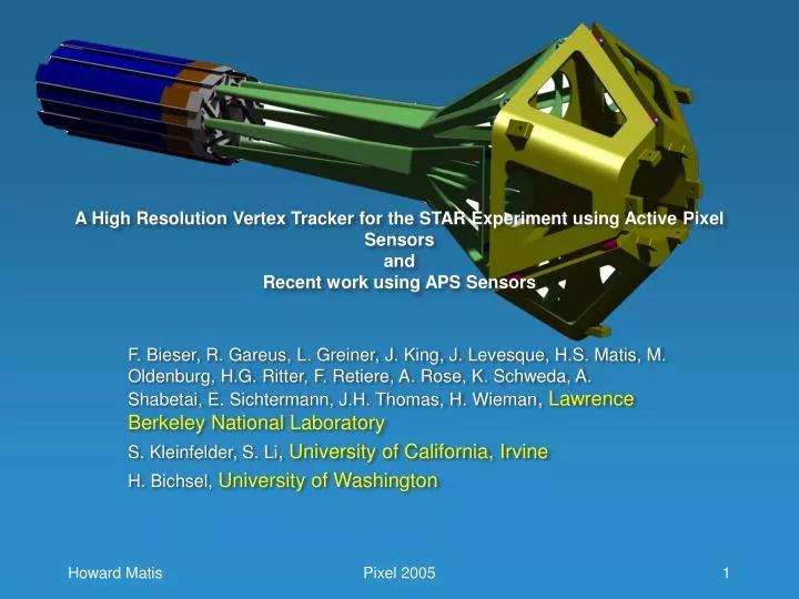
A High Resolution Vertex Tracker for the STAR Experiment using Active Pixel Sensors andRecent work using APS Sensors F. Bieser, R. Gareus, L. Greiner, J. King, J. Levesque, H.S. Matis, M. Oldenburg, H.G. Ritter, F. Retiere, A. Rose, K. Schweda, A. Shabetai, E. Sichtermann, J.H. Thomas, H. Wieman, Lawrence Berkeley National Laboratory S. Kleinfelder, S. Li, University of California, Irvine H. Bichsel,University of Washington Pixel 2005
PART I - DETCTOR physics motivation for a thin vertex detector deconfinement u-, d-quarks and ‘bound-states’ gain mass • Study initial properties of a nuclear collision • u, d, s quarks gain mass become thermalized • Final state effects • Measures later/cooler times of the collision • d, b quarks produced at early time • Intrinsic mass • Measure of early collision Phase and Chiral transitions • Need to measure particles above 0.5 GeV/c • High collision density - more than 2000 tracks • Measures secondary particles >100 µm from collision point Pixel 2005
detector requirements • Study D0 measurement • Multiple scattering in beam pipe sets fundamental limits • “Dream” Detector • Thickness 240 µm Si equivalent • Position resolution 8 µm Pixel 2005
star micro vertex detector • Two layers • 1.5 cm radius • 4.5 cm radius • 24 ladders • 2 cm 20 cm each • < 0.3% X0 • ~ 100 Mega Pixels Pixel 2005
close-up view Pixel 2005
sensor • Sensor under development at IReS • First prototype made using 0.25 µm process by TSMC • Second version in production using 0.35 µm by AMS Pixel 2005
ladder • 10 thinned APS detectors • Top of a matching row of thinned readout chips • Three-layer aluminum Kapton cable • Silicon cable structure is bonded to a carbon composite v, closing the beam to make a rigid structure • Wire bonding to the cable Pixel 2005
ladder 2 carrier candidates – X0 =0.11 % Top layer = 50 µm CFC Middle layer = 3.2 mm RVC Bottom layer = 50 µm CFC Outer shell = 100 µm CFC (carbon fiber composite) Fill = RVC (reticulated vitreous carbon foam) Pixel 2005
ladder prototypes • Mechanical Prototype with 4 MIMOSA-5 detectors glued to the Kapton cable assembly. Tested for • Vibration • Stiffness • A prototype cable (Cu) has been designed, constructed and tested. • Prototype ladder using thinned 50 µm MIMOSA-5 detectors. Currently under test with DAQ Pixel 2005
heavy flavor tracker (hft) parameters Pixel 2005
mechanical requirements • Geometry • Maintain position resolution of ~ 10 µm • Low mass / radiation length (X0~ 0.3% / layer) • Coverage of -1 < < 1 • Function • Easy to calibrate • Easy to align • Easy to remove, repair and replace electronics (ladders will need to have a local survey) • Fit easily into the existing detector and infrastructure at STAR Pixel 2005
conceptual mechanical design • Mounted to SVT cone • Slides in and out on one end • Ladders moves as beam pipe diameter increases Pixel 2005
kinematic support structure • Support bolts unto STAR • Green structure provides stable support for the ladder • Three point kinematic mounts assure accurate positioning • Can move detector in and out with reproducibility Pixel 2005
PART II - APS RESEARCH studies with scanning electron microscope • Access to 5 - 30 keV scanning electron microscope • Thought needed to punch through 2-3 µm • Believed could detect these electrons 12 µm 30 keV electrons Pixel 2005
cross sectional view(Tilt at 520) Pt Layer Top of IC Artifact dueto charge Top coating Epi-layer Pixel 2005
element analysis Pt Al Si Ti O Ga W Pixel 2005
30 kev electrons do not penetrate to the epilayer Pixel 2005
µm can detect “electrons” with reasonable accuracy • Can see microscope • Measuring Bremsstrahlung • Maximum intensity ~3000 /frame • Evaluate charge sharing of cell • Evaluate position resolution algorithms • Best Pixel 2005
track efficiency is critical with noise level • Monte Carlo study two different algorithms with MIMOSA 5 • Look for seed pixels • Smooth data and then look for seed pixels • Real pedestal data with imbedded electron spectrum • Efficiency algorithm dependent • Algorithm choice dependent on noise Pixel 2005
how much signal do you get out of an aps sensor? Bichsel & Saxon • Calculations show that energy loss in thin materials much less than thicker • Bichsel & Saxon, Phys. Rev. A11, 1286 (1975). • Observed in aluminum • Perez & Sevely, Phys. Rev. A 16, 1061 (1977). Landau Energy Deposited - eV 0.76 µm Al 1 MeV e- Pixel 2005
study at lbnl advanced light source • Study 1.5 GeV/c electrons • Calculated expected energy • Use Bichsel formalism • 0.25 µm TSMC • 8 µm epitaxial layer • Need to shift theory by 1.5 for good agreement Pixel 2005
p-well MIP n-well P epitaxial layer p++ substrate some checks • Epitaxial (epi) layer 8 µm (error perhaps 1 µm) • Use Bichsel formalism on 8.5 µm aluminum data • 1.66 keV scales to 1.43 keV silicon (most probable) • Bichsel predicts • 1.43 keV • Total systematic error 10 - 20 % • Cannot explain 50% excess epitaxial layer Pixel 2005
p-well MIP n-well P epitaxial layer p++ substrate a hypothesis • Extra charge equivalent to 4 µm • Electrons could be coming from upper p-well and p++ substrate • Check with Mimosa-5 data (AMS 0.6 µm) • Most Probable - 996 e- • Bichsel - 746 e- • Equivalent to extra 4.7 µm over nominal 14 µm Pixel 2005
5 10 5 10 20 20 30 30 Log Scale Linear Scale scaling of cell size • UCI design a multi-spacing chip • 5 µm, 10 µm, 20 µm and 30 µm • All cell sizes on one chip • Minimize systematic errors • Charge sharing very similar • Can see small absorption of charge in epitaxial layer • Good scaling Pixel 2005
summary • Proposal for a vertex detector with APS technology • Awaiting funding • Transmission scanning microscopes can be used to probe sensors • Software algorithms important to get high hit reconstruction - choice very sensitive to absolute noise • Cell scales from 5 to 30 µm • More charge then expected coming from APS Pixel 2005
A Heavy Flavor Tracker for STAR Z. Xu Brookhaven National Laboratory Y. Chen, S. Kleinfelder, A. Koohi, S. Li University of California, Irvine H. Huang, A. Tai University of California, Los Angeles V. Kushpil, M. Sumbera Nuclear Physics Institute AS CR C. Colledani, W. Dulinski, A. Himmi, C. Hu, A. Shabetai, M. Szelezniak, I. Valin, M. Winter Institut de Recherches Subatomique, Strasbourg M. Miller, B. Surrow, G. Van Nieuwenhuizen Massachusetts Institute of Technology F. Bieser, R. Gareus, L. Greiner, F. Lesser, H.S. Matis, M. Oldenburg, H.G. Ritter, L. Pierpoint, F. Retiere, A. Rose, K. Schweda, E. Sichtermann, J.H. Thomas, H. Wieman, E. Yamamoto Lawrence Berkeley National Laboratory I. Kotov Ohio State University Pixel 2005
end Pixel 2005
backup slides Pixel 2005
precision tie points coupling the hft system to the star support cone Pixel 2005
thin beam pipe • Central beryllium region • 14.5 mm radius • 10 beam size • 500 µm thick walls • Outer region • 30 mm radius aluminum • Exoskeleton caries load Pixel 2005
end view showing the hft ladders between spokes of the inner beam pipe support Pixel 2005
data flow and processing stages in the readout chip • Each stage can be bypassed to allow raw or partially unprocessed data to be routed to the DAQ • The first stage is a CDS preprocessor which is followed by pedestal subtraction and a pixel masking filter • Further processing allows us to sum up the value of 1, 4 or 9 pixels before a threshold cut is applied. • The last stage includes zero suppression and transcoding to hit positions. Pixel 2005
readout layout • sketch of the readout-topology on a detector ladder • one of ten APS and the corresponding readout chip layout. Pixel 2005
rdo asic • ADC – 10 bit ADC for signals from sensor chip • CDS – Chip will perform correlated double sampling • High speed LVDS output • Configuration, control, clock, synch functions • Both chips thinned to 50 µm thickness. • X0 = 0.053 % each Pixel 2005
daq ladders can be combined to one optical link. Figure5: Pixel 2005
hit loading Pixel 2005
Comparison with mimosa-5 Pixel 2005
material budget Pixel 2005
using an aps as a camera Pixel 2005