Download
1 / 26
290 likes | 520 Views
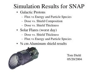
Ceramic Focal Plane Components For SNAP B. C. Bigelow, UM Physics 4/13/05. Ceramic Detector Packages. AlN detector package material already demonstrated Ground and space heritage well established Cryo epoxies known, package assembly procedures established

E N D
Ceramic Focal Plane Components For SNAPB. C. Bigelow, UM Physics4/13/05
Ceramic Detector Packages • AlN detector package material already demonstrated • Ground and space heritage well established • Cryo epoxies known, package assembly procedures established • See Oluseyi, Bercovitz, et. al. (LBNL) • Package assembly to set height, flatness to ~ +/- 5 microns • See Miyazaki, et al, PASJ • AlN CTE close match to Si, SiC, Invar • Natural match to Si CCD sensor material • Near-match to HgCdTe Si MUX material • Can be machined, polished, epoxy-inserted, etc. • AlN -> near match for SiC • SiC package material base-lined for GAIA mission • More later! Bruce C. Bigelow -- UM Physics
CTE for Focal Plane Materials • CTE plot courtesy of Pat Jelinsky: Bruce C. Bigelow -- UM Physics
Subaru Suprime Camera • On Subaru 8.2m telescope, Mauna Kea, Hi • See Miyazaki, et al • 5 x 2 mosaic of LL-MIT 2K x 4k CCDs - 83 Megapixels • AlN CCD packages • AlN cold-plate • Assembled mosaic is flat to approx. +/- 5 microns • Threaded studs epoxied into AlN packages • Flat interface between packages and cold-plate Bruce C. Bigelow -- UM Physics
Subaru Suprime Camera Miyazaki, et al Bruce C. Bigelow -- UM Physics
Subaru Suprime Camera AlN cold-plate 120mm x 150mm mosaic Bruce C. Bigelow -- UM Physics
Subaru Suprime Camera AlN package and “buffer block” Stud is epoxied into AlN buffer block Bruce C. Bigelow -- UM Physics
Subaru Suprime Camera AlN buffer block and spacer shims in assembly jig Bruce C. Bigelow -- UM Physics
Subaru Suprime Camera AlN CCD package epoxied to buffer block Bruce C. Bigelow -- UM Physics
GAIA mission SiC focal plane • Boostec SiC material: • Sintered fabrication process • Less than 3% porosity • Pure, alpha phase SiC, no free silicon • Boostek SiC Moly • Density: 3100 kg/m^3 10,200 kg/m^3 • Young’s modulus: 420 GPa 330 GPa • Flexural strength: 450 Mpa 415 Mpa • CTE (room temp): 4.0 PPM/C 5.35 PPM/C • Thermal conductivity: 180 W/m·k 138 W/m·k Bruce C. Bigelow -- UM Physics
GAIA mission SiC cold-plate Boostec/Astrium GAIA focal plane demonstrator model: Sintered SiC, 770mm by 580mm by 36mm, 8kg. Bruce C. Bigelow -- UM Physics
GAIA mission SiC cold-plate GAIA cold-plate - detector mounting detail. Note finished bores on mounting holes Bruce C. Bigelow -- UM Physics
Ceramic CCD Packages for SNAP • CCD package features: • All dimensions and mounting features per ICD 00065-AC14A (HDH) • Hypertonics KA series connectors per ICD • All vented hardware – but not always shown! • AlN PCB interfaces between detectors and connectors • Integral filter/aperture assemblies • AlN or SiC package and mount material (interchangeable) Bruce C. Bigelow -- UM Physics
Ceramic CCD package Invar inserts with internal threads for M3 mounting screws Bruce C. Bigelow -- UM Physics
Ceramic CCD package Round insert, diamond insert, undersized insert provide kinematic constraint of in-plane DOF – X, Y, and rot Z. Ground pads define tip, tilt, and piston of package Bruce C. Bigelow -- UM Physics
Ceramic CCD assembly AlN or SiC mount AlN or SiC CCD package epoxy Ribbon cable Invar insert, epoxied in PCB Invar insert, epoxied in Hypertronics KA series, 72 pins Bruce C. Bigelow -- UM Physics
Ceramic CCD package CTE-matching filter frame, with filter and aperture mask Bruce C. Bigelow -- UM Physics
Ceramic MCT Packages • MCT package features: • All dimensions and mounting features per ICD 00065-AC14A (HDH) • Hypertonics KA series connectors per ICD • All vented hardware – but not always shown! • AlN PCB interfaces between detectors and connectors • Integral filter/aperture assemblies • AlN or SiC package and mount material (interchangeable) Bruce C. Bigelow -- UM Physics
Ceramic MCT package Near-copy of CCD PCB, but wraps around for wire-bonding to sensor MUX on top surface AlN/SiC PCB isolates detector package from connector thermal stresses Bruce C. Bigelow -- UM Physics
Ceramic MCT package Bruce C. Bigelow -- UM Physics
Ceramic MCT package Filter frame clearance for wire-bonds Bruce C. Bigelow -- UM Physics
Ceramic MCT package Bruce C. Bigelow -- UM Physics
SNAP ¼ CCD+MCT mosaic CCD MCT Bruce C. Bigelow -- UM Physics
SNAP ¼ CCD+MCT mosaic Section showing mounting interface details Bruce C. Bigelow -- UM Physics
SNAP ¼ CCD+MCT mosaic Section showing mounting interface details Bruce C. Bigelow -- UM Physics
SNAP ¼ CCD+MCT mosaic Back side of FP mosaic showing mounting screws and access to connector Bruce C. Bigelow -- UM Physics