Download
1 / 24
250 likes | 420 Views
Combinational Logic Design. digital systems are complex and sophisticated. Millions of gates. It is impossible to design each and every implementation of functions from scratch. Even seemingly simple expressions may turn out to have not so simple implementations.

E N D
Combinational Logic Design digital systems are complex and sophisticated Millions of gates It is impossible to design each and every implementation of functions from scratch. Even seemingly simple expressions may turn out to have not so simple implementations. Fortunately, many expressions are compositions of expressions we know and whose implementations we can re-use and combine. Digital design Ed F. Deprettere Leiden University
Design a circuit with nine inputs and one output: if number of 1’s in input is odd (even) then output is 1 (0) F(0, 0, 0, 0, 0, 0, 0, 1, 1) = 0 F(1, 0, 1, 0,1,0,0,0,0)= 1 What about the truth table? It has29 = 512 rows (!) 50% of these will have an odd number of 1’s : 256minterms(!) It turns out thatall minterms are prime! Conclusion: 9x256 = 2304 literals! Example: 9-input Odd Parity Generator Digital design Ed F. Deprettere Leiden University
n Half the number of minterms (2 /2) have an odd number of 1’s XYZ+XYZ+XYZ+XYZ and they all appear in the SOP form of the many-variable XOR Y An odd number of variables must be 1 No symplification is possible! 1 1 1 X 1 Z Parity generator and parity checker Recall XOR function: X Y Z = m(1, 2, 4, 7) Such functions are special. They are called Odd Functions. Why? Parity GeneratorP = X Y Z Parity CheckerC = X Y Z P MESSAGE = (X,Y,Z,P) Total number of 1’s even Digital design Ed F. Deprettere Leiden University
XOR(X,Y) computes odd parity of two inputs (X, Y) XOR(XOR(X, Y), Z) computes odd parity of three inputs (X,Y,Z) Thus, odd parity of 9 inputs is generated by: X 0 X 1 X 2 X 3 X 4 X 5 X 6 X 7 X 8 Example: 9-input Odd Parity Generator (cont’d) Digital design Ed F. Deprettere Leiden University
Combinational Logic Design How to design combinational circuits? Use fundamental circuits called basic blocks Re-usebasic blocks to design new circuits Use hierarchy Use toolsfor Computer Aided Design Digital design Ed F. Deprettere Leiden University
System Diagram Circuit Design for Unit Circuit Symbol for Unit Logic Diagram for Module Example: The 9-variable PG Digital design Ed F. Deprettere Leiden University
Design Procedure Requirements (Input-Output) and Constraints Specification Truth Table of Function for Requirements Optimization (transformations) to meet constraints Implementation Logic diagram using ANDs, ORs, and NOTs Technology mapping Equivalent diagram based on available cell library Verification Diagram’s Output, given Inputs equals the requirements. Digital design Ed F. Deprettere Leiden University
Example Requirement and Constraint One-bit adder; three-level. Specification Digital design Ed F. Deprettere Leiden University
X Y S C Z 1-bit adder S = X’Y’Z + X’YZ’ + XY’Z’ + XYZ = XOR(X,Y,Z) C = XY + Z(XOR(X,Y)) (use maps) Digital design Ed F. Deprettere Leiden University
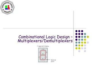
(Seven-Segment) (BCD) (4) 0 1 0 0 Other Examples BCD-to-Excess-3 Code Converter Excess-3(Decimal) = Binary(Decimal + Decimal(3)) Decimal = 8 8 + 3 = 11 Excess-3(8) = 1011 See Lab Hands-on BCD-to-Seven-Segment Decoder Digital design Ed F. Deprettere Leiden University
A circuit is designed to inplement a function. Question: is the design correct? Answer: find the circuit’s actual input-ouput relation and see whether it is the desired function. How? 1. Label gate outputs that depend on input variables directly 2. Write Boolean functions for these gate outputs 3. Repeat process until final output is obtained Verification Alternatively: build up Truth Table instead of function. Digital design Ed F. Deprettere Leiden University
Finding the circuit’s function T1=B'C T2=A'B B'D T3=T1+A=A+B'C F2 = T5 = A'B + D Digital design Ed F. Deprettere Leiden University
Write input rows (2n, where n is the number of inputs) 2. Break circuit up into blocks, label each block with symbol 3. Obtain truth table for blocks with functions that depend on input variables only 4. Go on to obtain truth table for blocks with functions that depend on previously defined inputs and block outputs, until columns for all circuit outputs are found. Truth Table from Circuit Digital design Ed F. Deprettere Leiden University
Example: Circuit to Truth Table Digital design Ed F. Deprettere Leiden University
Circuit to Truth Table (cont’d) Digital design Ed F. Deprettere Leiden University
Technology Mapping Custom Design The best you can, using just transistors. Time consuming and expensive Standard-Cell Design Re-use of cells in library. Faster, but sub-optimal Gate-Array Design Pre-fabricated chips with millions of gates. All that is to be done is connect the gates. Very fast and to-day’s preferred Gate Arrays are mature forms of Programmable Logic Digital design Ed F. Deprettere Leiden University
“Programmable” Programmable Logic In general, Programmable Logic Array (PLA) consist of two arrays: An AND array, and An OR array. Array logic Two-input AND OR array AND array Three-input OR Digital design Ed F. Deprettere Leiden University
2 • Programmable Read-only memory • (PROM, EPROM, E PROM) Types • AND array is fixed (decoder), OR array is • programmable • AND array is programmable, OR array is fixed • 3. AND array and OR array are programmable The names: programmable logic devices: 2.Programmable array logic (PAL) devices 3. Programmable logic array (PLA) devices Digital design Ed F. Deprettere Leiden University
k k A 2 n ROM stores 2 words of n bits each in a nonvolatile way. k It consists of 1) a k-to-2 decoder and 2) a programmable OR array 0 1 2 . . . 31 0 1 2 3 4 5-to-32 decoder 7 6 5 4 3 2 1 0 To be considered as having 32 inputs Each decoder out connected to one of the inputs of each OR gate 32 lines = 32 inputs/OR, 8 ORs 32 8=256 programmable connections. Read-only Memory (ROM) Address in Data out Digital design Ed F. Deprettere Leiden University
XYZ F1 F2 F3 F4 (= Memory Word) 000 001 000 01 0000 001 000 010 00 0101 010 011 100 10 0000 011 000 100 00 0010 100 010 000 11 1100 Three bits three bits three bits two bits four bits 12 bits 0 1 2 3 4 x x 3-to-8 decoder ROM design Is a Truth table Digital design Ed F. Deprettere Leiden University
P-term 1 connected P-term 2 connected P-term 3 not connected P-term 4 connected Out is F1 (not F1) k m prog. connects F1 = AB + AC + ABC F2 = AC + BC 2n k progr. connects 1 AB Inputs Outputs (T) (C) Product terms A B C F1 F2 1 1 0 1 2 1 1 1 1 3 1 1 1 4 0 1 0 1 AC 2 BC 3 ABC 4 0 1 F1 C C B B A A A connected B connected C not connected F2 Prog’able Logic Array (PAL) In a PLA, the decoder of the PROM is replaced by an AND array. The AND array generates product terms. k P-terms (four) PLA Programming table. n inputs (three) When programmable by user, PLA is called field programmble. m outputs (two) Digital design Ed F. Deprettere Leiden University
programmable One buffer/inverter input One buffer/inverter output feedback One output A k-wide AND-OR array (k programmable AND gates and one fixed OR gate) four programmable AND gate connections, Prog’able Array Logic (PAL) In these programmable devices, the OR array is fixed. PALs are composed of a number of PAL sections. Out Each section consists of: In Product terms cannot be shared among sections. Thus each output (function) can be simplified by itself (unlike in PALs where you want to share product terms). The number of P-terms in a section is fixed. If you need more, use more sections. Digital design Ed F. Deprettere Leiden University
Address MUX2 MUX1 MUX0 A2 A1 A0 M2 M1 M0 0 0 0 1 0 1 0 0 1 1 1 1 0 1 0 1 0 1 0 1 1 0 1 0 1 0 1 1 1 1 1 1 0 0 0 1 MUX2 = m(0, 1, 2, 4) = A 2 A0 + A 1A0 MUX1 = m(1, 3, 4) = A 2A0 + A 1A0 A2 A2 A1 A1A0A0M2M2 MUX0 = m(0, 1, 2, 4,5) = MUX2 + A 1A0 1 A2 M0 2 P-term A2 A1 A0 M2 Output 1 1 2 1 0 M0 3 0 1 4 0 0 M1 5 0 0 6 0 1 M2 3 A1 M1 4 5 A0 M2 A2 connected A1 not connected A0 connected 6 Example. PAL Programming Table. Digital design Ed F. Deprettere Leiden University
FPGAs Most popular are Xilinx and Altera. See your hands-on exercise implementations. I’ll come back to them when we have seen sequential circuits. Programming FPGAs is all you have to master to realize even very complicated digital systems That’s exactly what you will master by the end of the course. Digital design Ed F. Deprettere Leiden University