Download
1 / 9
90 likes | 172 Views
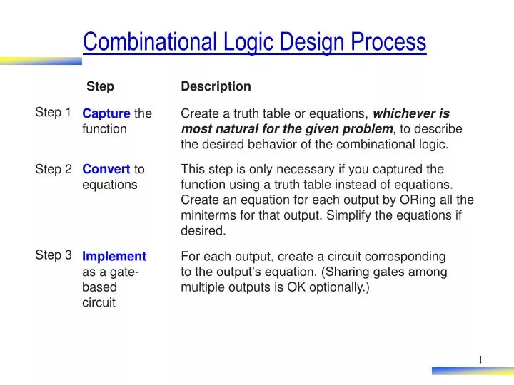
Combinational Logic Design Process. Step. Description. Step 1. Capture the function . Create a truth table or equations, whichever is most natural for the given problem , to describe the desired behavior of the combinational logic. Step 2. Convert to equations.

E N D
Combinational Logic Design Process Step Description Step 1 Capture the function Create a truth table or equations, whichever is most natural for the given problem, to describe the desired behavior of the combinational logic. Step 2 Convert to equations This step is only necessary if you captured the function using a truth table instead of equations. Create an equation for each output by ORing all the miniterms for that output. Simplify the equations if desired. Step 3 Implement as a gate-based circuit For each output, create a circuit corresponding to the output’s equation. (Sharing gates among multiple outputs is OK optionally.)
a abc b c bcd d cde e y def f efg g fgh h Example: Three 1s Detector • Problem: Detect three consecutive 1s in 8-bit input: abcdefgh • 00011101 1 10101011 0 11110000 1 • Step 1: Capture the function • Truth table or equation? • Truth table too big: 28 = 256 rows • Equation: create terms for each possible case of three consecutive 1s • y = abc + bcd + cde + def + efg + fgh • Step 2: Convert to equation -- already done • Step 3:Implement as a gate-based circuit
a b c a b c a b c a y z b c a b c a b a b c Example: Number of 1s Count • Problem: Output in binary on two outputs yz the number of 1s on three inputs • 010 01 101 10 000 00 • Step 1: Capture the function • Truth table or equation? • Truth table is straightforward • Step 2: Convert to equation • y = a’bc + ab’c + abc’ + abc • z = a’b’c + a’bc’ + ab’c’ + abc • Step 3:Implement as a gate-based circuit
NAND NOR XOR XNOR x x F F y y x y F x y F x y F x y F 0 0 1 0 0 1 0 0 0 0 0 1 0 1 1 0 1 0 0 1 1 0 1 0 1 0 1 1 0 0 1 0 1 1 0 0 1 1 0 1 1 0 1 1 0 1 1 1 More Gates • NAND: Opposite of AND (“NOT AND”) • NOR: Opposite of OR (“NOT OR”) • XOR: Exactly 1 input is 1, for 2-input XOR. (For more inputs -- odd number of 1s) • XNOR: Opposite of XOR (“NOT XOR”)
d0 d0 d0 d0 1 0 0 0 d1 d1 d1 d1 i0 i0 i0 i0 0 1 0 0 0 1 0 1 d0 0 0 1 0 i1 i1 i1 i1 0 0 1 1 d2 d2 d2 d2 d1 d3 0 d3 0 d3 0 d3 1 d2 i1’i0’ d3 i1’i0 i1i0’ i1 i0 i1i0 Decoders and Muxes • Decoder: Popular combinational logic building block, in addition to logic gates • Converts input binary number to one high output • 2-input decoder: four possible input binary numbers • So has four outputs, one for each possible input binary number • Internal design • AND gate for each output to detect input combination A decoder decodes an input n-bit binary number by setting exactly one of the decoder’s 2n outputs to 1.
2 1 0 2 1 0 1 0 0 0 0 1 1 0 0 1 0 0 0 0 0 0 0 1 0 0 0 0 0 0 0 0 0 0 0 0 0 0 0 0 0 0 Decoder Example • New Year’s Eve Countdown Display • Microprocessor counts from 59 down to 0 in binary on 6-bit output • Want illuminate one of 60 lights for each binary number • Use 6x64 decoder • 4 outputs unused Happy 0 New Year i0 d0 i1 d1 1 i2 d2 2 3 i3 d3 essor c i4 o r i5 op r ic d58 M e d59 d60 58 d61 59 6x64 d62 dcd d63
Multiplexor (Mux) • Mux: Another popular combinational building block • Routes one of its N data inputs to its one output, based on binary value of select inputs • 4 input mux needs 2 select inputs to indicate which input to route through • 8 input mux 3 select inputs • N inputs log2(N) selects • Like a railyard switch
× 2 1 1 i0 d i1 0 s0 1 i0 d i1 i0 × 4 1 i0 i1 s0 i1 d d i2 i2 i3 i3 s1 s0 4x1 mux s1 s0 Mux Internal Design i0 (1*i0=i0) × × 2 1 2 1 i0 (0+i0=i0) i0 i0 0 d d i1 i1 s0 s0 0 2x1 mux 0 An Mx1 multiplexer has M data inputs and one output, and allows only one input to pass through to that output. A set of select inputs determines which input to pass through.
Additional ConsiderationsNon-Ideal Gate Behavior -- Delay • Real gates have some delay • Outputs don’t change immediately after inputs change