Download
1 / 33
330 likes | 480 Views
Module 4: Metrics & Methodology Topic 1: Synchronous Timing. OGI EE564 Howard Heck. Where Are We? . Introduction Transmission Line Basics Analysis Tools Metrics & Methodology Synchronous Timing Signal Quality Source Synchronous Timing Recovered Clock Timing Design Methodology

E N D
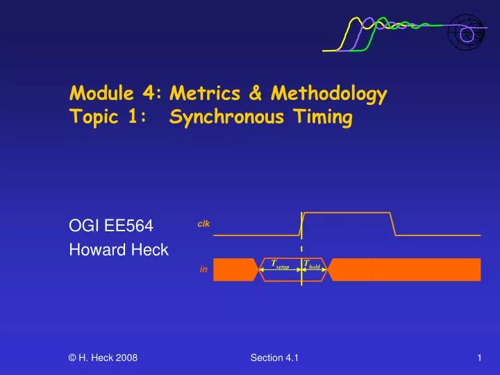
Module 4: Metrics & MethodologyTopic 1: Synchronous Timing OGI EE564 Howard Heck Section 4.1
Where Are We? • Introduction • Transmission Line Basics • Analysis Tools • Metrics & Methodology • Synchronous Timing • Signal Quality • Source Synchronous Timing • Recovered Clock Timing • Design Methodology • Advanced Transmission Lines • Multi-Gb/s Signaling • Special Topics Section 4.1
Contents • Synchronous Memory Elements • Operation • Timing Requirements • Bus Operation • Clock Skew & Jitter • Timing Analysis – Setup and Hold • Manufacturability Considerations • System Timing Equations • Summary Section 4.1
Synchronous Memory Elements - Operation Operation • A data signal (in) that is present at the input to the flip-flop is “latched” into the flip-flop by the rising edge of the input clock signal (clk). • On the next rising edge of clk, the data signal is released to the output of the flip-flop (out). Section 4.1
Synchronous Memory Elements - Timing Timing • Valid data must be present for a minimum amount of time prior to the input clock edge to guarantee successful capture of the data. This is setup time, Tsetup. • Data must remain valid for a minimum amount of time after the input clock edge to guarantee that the proper value is captured. This is the hold time, Thold. Section 4.1
Synchronous Bus Operation clk • We use the clock to control the transmission of data from the latch in the source (a) to the latch in the destination (b). CLK CLK CORE TO CORE FROM Q Q D D a b • The initial clock pulse causes the source latch to release the data onto the interconnect. • The next clock pulse causes the destination latch to capture the data that was transmitted on the interconnect • We have 1 full clock cycle to get the data from ato b. Section 4.1
Synchronous Signaling Sequence CLK @ A T (a) drv_clk (1a) T (a) prop_clk (1b) clk • Initial (driving) clock pulse transmission from clock generator to source. CLK CLK CORE CORE TO FROM Q Q D D a b • Tdrv_clk(a) = delay of the clock buffer circuit connected to the source (a). • Tprop_clk(a) = delay of the interconnect that between clk & a. Section 4.1
Synchronous Signaling Sequence CLK @ A Data @ A Data @ B T (a) drv_clk (1a) T (a) prop_clk (1b) T prop (2b) T T drv setup (2a) (2c) clk • Data transmission from source to destination. CLK CLK CORE CORE TO FROM Q Q D D a b • Tdrv = delay of the output buffer circuit for the data signal. • Tprop= interconnect delay between source and destination. • Tsetup= delay of the input buffer plus the flip-flop setup requirement. Section 4.1
Synchronous Signaling Sequence CLK @ A Data @ A Data @ B T (a) T (b) drv_clk drv_clk (1a) (3a) CLK @ B T (a) T (b) prop_clk prop_clk (1b) (3b) T prop (2b) T T drv setup (2a) (2c) clk • Second (receiving) clock pulse transmission from clock generator to destination. CLK CLK CORE CORE TO FROM Q Q D D a b • Tdrv_clk(b) = delay of the clock buffer circuit connected to b. • Tprop_clk(b) = delay of the interconnect between clk & b. Section 4.1
Clock Skew • What happens if the clock signals at the source and destination are not in phase? • What if the clock arrives at the destination before it reaches the source? Vice-versa? • What are the sources of uncertainty in the phase relationship between different clock signals? Section 4.1
Clocks Skew CLK @ A Data @ A Data @ B Z0, td CL Tdrv a Clock Driver Z0, td Tdrv CL b • Clock Skew: pin-to-pin variation in the timing of input clock at each agent (source & destination, in our example) on a bus. • The net effect of clock skew is that it can • reduce the total delay that signals are allowed to have for a given frequency target. • require larger minimum signal delays in order to avoid logic errors. (We’ll cover this in more detail shortly.) • Clock skew is caused by: • variation between the clock driver circuits in a given part (Tdrv). • variation in the loading between different agents on the bus (CL). • variation in interconnect characteristics (Z0, td). CLK @ B Section 4.1
Clock Jitter IDEAL JITTER ACTUAL T - T T + T T T + T T - T T - T cycle jitter cycle jitter cycle cycle jitter cycle jitter cycle jitter Pulse Width (Ideal) Pulse Width (Actual) What it is: Cycle-to-cycle variation in the clock period. Section 4.1
Clock Jitter – Causes & Effects CLK @ A Data @ A Data @ B CLK @ B • The net effect of clock jitter is that it can reduce the total delay that signals are allowed to have for a given frequency target. • i.e. jitter can reduce the clock cycle time, as illustrated by the diagrams on the previous page. • Clock jitter is caused by: • noise in the system that affects the response of the clock driver circuits. • noise in the system that affects the transmission characteristics of the signals. • Since they affect the operation we must consider clock skew and jitter in our timing analysis. Section 4.1
Skew & Jitter Example 10ns 0.25ns 0.25 ns 9.5ns • 100 MHz bus • Min clock period = 10 ns • Given: • Max skew = 250 ps • Max edge-edge jitter = 250 ps. CLK @ A CLK @ B • Calculate the minimum effective clock period: • minimum effective period = minimum period – maximum skew – maximum jitter • min effective period = 10.0 ns – 0.25 ns – 0.25 ns = 9.5 ns • Therefore, maximum allowed for silicon plus interconnect delay is 9.5 ns. Section 4.1
Setup Timing T cycle T skew T drv T prop T setup T jitter • We need to constrain the data delay such that it makes the trip from source to destination in time to meet setup requirements – while accounting for clock uncertainty. CLK @ A Data @ A Data @ B CLK @ B [4.1.1] For a rigorous derivation see Appendix A. Section 4.1
Hold Timing T drv T prop T skew hold • We need to constrain the data delay such that it does not arrive at the destination until the hold requirement is met – while accounting for clock uncertainty. CLK @ A Data @ A Data @ B T CLK @ B [4.1.2] Section 4.1
Manufacturability Considerations • Sources of variability in silicon: • manufacturing process (e.g. silicon gate length) • operating temperature (MOS speed as temp ) • operating voltage (MOS speed as voltage ) • Impact: variability leads to a range of values for driver and receiver timings • Example: Pentium® Pro GTL+ timings • Minimum driver valid delay = 0.55 ns • Maximum driver valid delay = 4.40 ns • Maximum receiver setup time = 2.20 ns • Maximum receiver hold time = 0.45 ns • Sources of interconnect variability: • Manufacturing variation (Z0, er) • Trace length variation (e.g. 144 signals for FSB) Section 4.1
Revised Timing Equations Setup Hold • Product specifications must comprehend the expected variation. • We need to modify the setup & hold equations: • The setup equation defines the minimum clock cycle time (max frequency) in terms of the maximum system delay terms. We want Tmargin_setup 0. • Excessive system delays can be handled by increasing cycle time, at the cost of reduced performance. • The hold equation defines minimum system delay requirements to avoid logic errors due to hold violations. We want Tmargin_hold 0. • Minimum delay violations cannot be fixed by increasing cycle time. Why? [4.1.3] [4.1.4] Section 4.1
Example: Pentium® II Processor 100 MHz Host Bus Timings Section 4.1
Synchronous Timing Summary • Synchronous memory elements require a stable data signal for a minimum amount of time prior to (SETUP) & after (HOLD) the input clock. • Hold and setup conditions determine the minimum and maximum system delays. • Setup and hold conditions can be analyzed by constructing timing loops in the timing diagrams. • Component delays exhibit variation across process and environmental conditions. Interconnect delays contain variations due to design and process. • Redefining driver and interconnect delays in terms of system and “spec” loads allows manufacturers to specify and test component delays. • System timing equations provide a key tool for examining trade-offs during system design. Section 4.1
References • S. Hall, G. Hall, and J. McCall, High Speed Digital System Design, John Wiley & Sons, Inc. (Wiley Interscience), 2000, 1st edition. • W. Dally and J. Poulton, Digital Systems Engineering, Cambridge University Press, 1998. • R. Poon, Computer Circuits Electrical Design, Prentice Hall, 1st edition, 1995. • H.B.Bakoglu, Circuits, Interconnections, and Packaging for VLSI, Addison Wesley, 1990. • H. Johnson and M. Graham, High Speed Digital Design: A Handbook of Black Magic, PTR Prentice Hall, 1993. • S. Dabral and T. Maloney, Basic ESD and I/O Design, John Wiley and Sons, New York, 1998. Section 4.1
Appendix A: Tco & Flight Time Return to main contents. Section 4.1
Device Specs and Test Loads W 65 10pF Spec Load System • Device specifications vs. system conditions • The manufacturer guarantees that the parts meet the values in the timing specifications when driving into the “spec load”. • The spec load is typically equal to the load presented to the device by the test environment. • This spec load is generally not the same as the load presented to the device by the system interconnect. Section 4.1
Impact of Spec Loads • Since the spec load is NOT equal to the load on the device when placed in a system: • An output buffer will have a different delay in the system than in the test environment. • To deal with this: • define new timing terms & • change the way we break the timings into separate components. Section 4.1
Flight Time Driver Pin into System Load Clock Input to Transmitting Chip Driver Pin into Test Load Tco Tflight Voltage Threshold Tdrv Tprop Receiver Pin Time Section 4.1
Flight Time Explained • Notice: • WedefinedTcoandTflightthis way to guarantee the overall system timings remain the same. • Define Tco (time from clock-in to data-out) as the delay from the input clock to the output data when driving into the test load. • Define Tflight (flight time) as the delay to the receiver minustheTco. • By defining the timings in this way, the flight time accounts for the propagation delay of the interconnect PLUS the difference between the driver delays when driving test load vs. the system load. Section 4.1
Another Perspective Problem: Solution: Section 4.1
Revised Timing Equations • The system designer relies on the synchronous timing equations help her/him define the working flight time window (min-to-max), given the component timing specs. • Ultimately, the equations provide a tool for the bus design team. • Use them to evaluate design trade-offs in order to achieve system performance (frequency) targets. Setup [4.1.5] Hold [4.1.6] Section 4.1
Appendix B: Synchronous Timing Equation Derivations Return to main contents. Section 4.1
Setup Timing Diagram & Loop Analysis Tcycle CLOCK @ clk input Tdrv_clk(a) CLOCK(a) @ clk output Tprop_clk(a) CLOCK(a) @ a Tdrv DATA @ a Tprop Tdrv_clk(b) Tmargin Tsetup DATA @ b CLOCK(b) @ clk output Tprop_clk(b) CLOCK(b) @ b Tjitter t [4.1.1a] Section 4.1 Return to main contents.
Setup Timing Equation • Setup equation • Define • Clock Delay [4.1.1a] [4.1.2a] • Clock Skew [4.1.3a] • Simplify [4.1.4a] Return to main contents. Section 4.1
Hold Timing Diagram & Loop Analysis CLOCK @ clk input Tdrv_clk(a) CLOCK(a) @ clk output Tprop_clk(a) CLOCK(a) @ a Tdrv DATA @ a Tprop DATA @ b Tdrv_clk(b) Tmargin_hold CLOCK(b) @ clk output Thold Tprop_clk(b) CLOCK(b) @ b t Section 4.1 Return to main contents.
Hold Timing Equation • Hold equation [4.1.5a] • Define • Clock Delay [4.1.6a] • Clock Skew [4.1.7a] • Simplify [4.1.8a] Return to main contents. Section 4.1