Download
1 / 27
270 likes | 275 Views
This article discusses the factors that limit the time resolution in gaseous detectors, including Pestov counters, resistive plate chambers, and micro-pattern gas detectors. It explores the physical origins of tails in the time response of spark counters and the benefits of thin gap and high-pressure systems. The time resolution of resistive plate chambers is parameterized and the advantages of multi-gap RPCs are highlighted. The article also covers the latest trends in micro-pattern gas detectors, including Micromegas and GEM technologies.

E N D
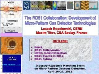
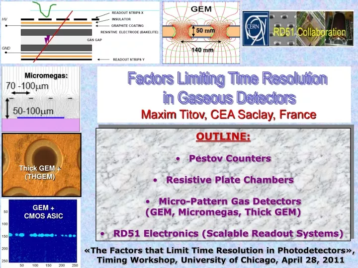
50 mm 140 mm Micromegas: Factors Limiting Time Resolution in Gaseous Detectors Maxim Titov, CEA Saclay, France • OUTLINE: • Pestov Counters • Resistive Plate Chambers • Micro-Pattern Gas Detectors • (GEM, Micromegas, Thick GEM) • RD51 Electronics (Scalable Readout Systems) Thick GEM + (THGEM) GEM + CMOS ASIC «The FactorsthatLimit Time Resolution in Photodetectors», Timing Workshop, University of Chicago, April 28, 2011
Yu. Pestov, NIM 196(1982)45 Spark (Pestov) Counter PHYSICAL ORIGIN OF TAILS IN THE TIME RESPONSE OF SPARK COUNTERS: GOOD TIME RESOLUTION ---> THIN GAP GOOD EFFICIENCY---> THICK GAS LAYER Yu Pestov et al. NIMA265 (1988) 198 Yu. Pestov et al., NIMA456 (2000) 11 Mangiarotti and A. Gobbi, NIMA. A482(2002)192 THIN GAP (100 µm) AND HIGH PRESSURES (~10 bar) HIGH RESISTIVITY ELECTRODE (PESTOV GLASS, 109 Ω cm HIGH-PRESSURE GAS VESSEL METAL CATHODE SEMI-CONDUCTING GLASS ANODE SIGNAL PICK-UP STRIPS Time resolution is proportional to discharge delay time(fluctuation of delay time is the sum of the fluctuation of the avalanche development and the occurrence of the streamer)
Resistive Plate Counters (RPC) READOUT STRIPS X HV INSULATOR GRAPHITE COATING HIGH RESISTIVITY ELECTRODE (BAKELITE) R. Santonico, NIMA 187(1981)37 P. Fonte, NIMA449 (2000) 295 ; P.Fonte, A.Smirnitski, C Williams, NIMA443(2000)201 I.Crotty et al, NIM A337(1994)370 GAS GAP GND READOUT STRIPS Y • Time resolution of a RPC can be parameterized as: • Δτ = λ/v • λ is the mean free path of electrons in avalanche, v is drift velocity of electrons • LOW λ and HIGH v can be obtained with dense/fast gas mixtures: C2H2F4 – iC4H10 – SF6 • Typical values: λ ~ 10μm, v ~ 100 μm/ns → Δτ ~ 100ps • Only avalanches within a few hundred mm from cathode generate signals • Raether limit: G = ed/λ < 108 → for λ ~ 10μm dgap ~ 200μm • To avoid discharges the gap must be reduced → MICROGAP
HV GND Resistive Plate Chambers (RPC) • INCREASING THE GAP PROVIDES BETTER EFFICIENCY PLATEAUX • For gas gaps of 0.3 mm or larger, the timing jitter in parallel-plate detectors • varies almost linearly with the width of the gaps DOUBLE GAP FWHM=1.7 ns SINGLE GAP FWHM 2.3 ns M. Abbrescia et al, NIM A431(1999)413
RPC Systems at the HEP Experiments (caveat - table last updated in 2003)
Multi Gap Resistive Plate Chambers Add boundaries that stop avalanche development. These boundaries must be invisible to the fast induced signal – induced signal on external pickup C. Williams, RD51 Mini-Week, July 20, 2010
HV GND Multi Gap Resistive Plate Chambers Would like large fast signal and small total charge (high rate capability) (After time correction using pulse-height) FLOATING • E. Cerron Zeballos et al, NIMA 374(1996)132 • Akindinov et al, NIMA 456(2000)16 C. Williams, RD51 Mini-Week, July 20, 2010
X readout strips 2 mm Bakelite r ~ 1010 Wcm 2 mm gas gap 2 mm Bakelite Y readout strips Pickup electrodes 0.4 mm glass plates 0.3 mm gas gaps Pickup electrodes Multi-Gap RPC for ALICE Experiment • Trigger RPC: R. Cardarelli, R. Santonico • ATLAS, CMS (~ 2000 – 4000 m2) timing resolution ~ 1-5 ns (MIPs) `Renaissance of particle identification’ using Multi-Gap RPC in ALICE: E ~ 50 kV Timing and Multi-Gap RPC ALICE TOF P. Fonte, V. Peskov, C. Williams (~50 ps) E ~ 100 kV
B 10 ps devices could be feasible – one of the biggest problem could be the electronics : the TDC C. Williams, RD51 Mini-Week, July 20, 2010
0.18 mm CMOS VLSI Ions 40 % 60 % Electrons Current Trends in Micro-Pattern Gas Detectors (Technologies) • Micromegas • GEM • Thick-GEM, Hole-Type Detectors and RETGEM • MPDG with CMOS pixel ASICs • Ingrid Technology CMOS high density readout electronics Micromegas MHSP Ingrid GEM THGEM
GEM (Gas Electron Multiplier) Thin metal-coated polymer foil chemically pierced by a high density of holes A difference of potentials of ~ 500V is applied between the two GEM electrodes. The primary electrons released by the ionizing particle, drift towards the holes where the high electric field triggers the electron multiplication process. I+ e- Induction gap e- S1 S2 S3 S4 Electrons are collected on patterned readout board. A fast signal can be detected on the lower GEM electrode for triggering or energy discrimination. All readout electrodes are at ground potential. 11 F. Sauli, Nucl. Instrum. Methods A386(1997)531 F. Sauli, http://www.cern.ch/GDD
Cartesian Compass, LHCb Small angle 33 cm Hexaboard, pads MICE Mixed Totem F. Sauli, NIM A386(1997) 531; F. Sauli, http://www.cern.ch/GDD Gas Electron Multiplier (GEM) Full decoupling of amplification stage (GEM) and readout stage (PCB, anode) Amplification and readout structures can be optimized independently ! Compass Totem NA49-future
GEM Time & Spatial Resolution: Single Photons Time-resolution is determined by the fluctuations in the photoelectron transit time from their emission point at the PC and, after multiplication, to the anode. depends on the detector geometry, the electric field conditions and properties of the gas composition, namely on the electron diffusion and drift velocity. Induction gap ~ 1mm Single Photon Time Resolution: Single Photon Position Accuracy: 200 µm low diffusion & high electron drift velocity in CF4 CF4 770 torr Intrinsic accuracy s (RMS)~ 55 µm FWHM ~160 µm Beam ~ 100 µm T. Meinschad et al, NIM A535 (2004) 324; D.Mormann et al., NIMA504 (2003) 93
GEM Time Resolution: Charged Particles Triple GEM for LHC-b Detector : Time Resolution ~ 5 ns Triple GEM for CMS Upgrade: • Time resolution for different • gas mixtures and gap configurations: • Ar(45):CO2 (15):CF4 (40) [gaps 3/1/2/1] • Ar(70):CO2(30) [gaps 3/2/2/2] G. Bencivenni, IEEE TNS 49(6), 3242 (2002) A. Bressan et al, Nucl. Instr. and Meth. A425 (1999) 262 A. Sharma, private communications
1,0E+07 1,0E+06 1,0E+05 1,0E+04 1,0E+03 Gain 1,0E+02 1,0E+01 MM = 330 NeCF4 10% MM = 290 NeCF4 5% 1,0E+00 DTHGEM NeCF4 10% DTHGEM NeCF4 5% 1,0E-01 1,0E-02 0 200 400 600 800 1000 D V THGEM (V) Thick-GEM Multipliers (THGEM) Simple & Robust Manufactured by standard PCB techniques of precise drilling in G-10 (and other materials) and Cu etching STANDARD GEM 103 GAIN IN SINGLE GEM THGEM 105 gain in single-THGEM • Other groups developed • similar hole-multipliers: • Optimized GEM: • L. Periale et al., • NIM A478 (2002) 377. • LEM: P. Jeanneret, • PhD thesis, 2001. 1 mm 0.1 mm rim to prevent discharges C. Shalem et al, NIMA558 (2006) 475; Double THGEM or THGEM/Micromegas • Effective single-electron detection • (high gas gain ~105 (>106) @ • single (double) THGEM) • Few-ns RMS time resolution • Sub-mm position resolution • MHz/mm2rate capability • Cryogenic operation: OK • Gas: molecular and noble gases • Pressure: 1mbar - few bar 106 C. Azevedo et al.; arXiv: 0909.3191
THGEM Time Resolution Signal shape is determined by the electron drift velocity and the width and field strength in the induction gap. • Smaller induction gap & • Higher electric field • Faster and narrower signals Single photons Time Resolution with MIPs: Electron drift time from THGEM surface into holes (simulation) Variations in rise-time, shape and amplitude (in addition to statistics of primary ionization) R. Alon et al., arXiv: 0809.4382 R. Alon, MsD 2007, Weinzmann Institute
MICro MEsh GAseous Structure (MICROMEGAS) Micromesh Gaseous Chamber: a micromesh supported by 50-100 mm insulating pillars Multiplication (up to 105 or more) takes place between the anode and the mesh and the charge is collected on the anode (one stage) Small gap: fast collection of ions Y. Giomataris et al, NIM A376(1996)29
Micromegas Time Resolution: Single Photons Single photon pulse height distribution (Polya) CsI coated mesh Excellent S/N performance: Single Photon Time Resolution: Micromegas Time Resolution : s ~ 700 ps Physical time jittersfor UV photons electron diffusion in the gas and noise. J. Derre et al., NIM A449 (2000) 314
The time information for each channel is extracted from the peak time of the ADC spectra. The strip with the earliest arrival time is taken as reference. A time resolution of ~1 ns results in space points with a resolution along the drift direction of ~50 μm T. Alexopoulos et al, NIM A617 (2010) 161
Deposit 0.8 µm Al grid 50 µm SU(8) Development of SU8 photoresist Pattern Al UV Exposure Micromegas + Timepix CMOS Pixel Chip ("InGrid") • InGrid: integrate Micromegas & pixel chip • by Si-wafer post-processing technology • Grid robustness & Gap/Hole accuracy “Ingrid” + Silicon Protection Layer: Apply Si3N4 (high resistivity layer 3-20 mm) for discharge quench & SPARK PROTECTION before InGrid production “InGrid” Detector: SiProt Layer M. Chefdeville et al, NIMA556(2006) 490
"InGrid" Detector: Single Electron Response and Discharges Observe electrons (~220) from an X-ray (5.9 keV) conversion one by one and count them in micro-TPC (6 cm drift) Study single electron response Provoke discharges by introducing small amount of Thorium in the Ar gas - Thorium decays to Radon 222 which emits 2 alphas of 6.3 & 6.8 MeV Round-shape images of discharges 1.5 cm Using low noise CMOS chips could lead to higher S/N -> help to improve time resolution Fe55 source P. Colas, RD51 Collab. Meet., Jun.16-17, 2009, WG2 Meeting M. Fransen, RD51 Collab. Meet., Oct.13-15, 2008, WG2 Meeting
RD 51 : Development of Micro-Pattern Gas Detector Technologies http://rd51-public.web.cern.ch/RD51-Public Collaboration of ~75 institutes worldwide, ~ 430 authors “RD51 aims at facilitating the development of advanced gas-avalanche detector technologies and associated electronic-readout systems, for applications in basic and applied research.” RD51 Collaboration Meetings: 1st - Amsterdam April 16-18, 2008 : http://indico.cern.ch/conferenceDisplay.py?confId=25069 2nd - Paris, October 13-15, 2008 : http://indico.cern.ch/conferenceDisplay.py?confId=35172 3rd - Crete (Greece), June 12-16, 2009 : http://candia.inp.demokritos.gr/mpgd2009/ 4th – CERN, November 23-25, 2009 : http://indicobeta.cern.ch/conferenceDisplay.py?confId=72610 5th – Freiburg, Germany, May 24-27, 2010 : http://indico.cern.ch/conferenceDisplay.py?confId=89325 6th – Bari (Italy), October 7-10, 2010: http://indico.cern.ch/conferenceDisplay.py?ovw=True&confId=102799 7th –CERN, April 12-15, 2011: https://indico.cern.ch/conferenceDisplay.py?confId=132080 22 Bari, Italy, October 2010 Freiburg , Germany, May 2010
RD51 Collaboration Organization GEM Consolidation around common projects:large area MPGD R&D, CERN/MPGD Production Facility, electronics developments, software tools, beam tests WG1: large area Micromegas, GEM; THGEM R&D; MM resistive anode readout (discharge protection); design and detector assembly optimization; large area readout electrodes and electronics interface WG2: double phase operation, radiation tolerance, discharge protection, rate effects, single-electron response, avalanche fluctuations, photo detection with THGEM and GridPix WG3: applications beyond HEP, industrial applications (X-ray diffraction, homeland security) WG4: development of the software tools; microtracking; neBEM field solver, electroluminescence simulation tool, Penning transfers, GEM charging up; MM transparency and signal, MM discharges WG5:MPGD Scalable Readout System (SRS); Timepix multi-chip MPGD readout WG6: CERN MPGD Production Facility; industrialisation; TT Network WG7: RD51 test beam facility 23
RD51 Project: Scalable Readout System (SRS) for MPGD • Development of a portable multi-channel readout system: • Scalable readout architecture: a few hundreds to several thousand channels • Suited for small test systems up to very large systems (> 100 k ch.) • Project specific part (ASIC) + common acquisition hardware and software
RD51 SRS General Readout Architecture • Scalability from small to large system • Common interface for replacing the chip frontend • Integration of proven and commercial solutions for a minimum of development • Default availability of a very robust and supported DAQ software package(DATE). Online/ Offline DATE Root-based offline Analysis DAQ HLT Test systems: LHC machine: 1000 BASE-SX up 500 m Multimode fiber (1 Gbit) 10 GBASE-SR up 300 m Multimode fiber ( 10 Gbit) GBE copper Trigger, clock and control Control PC Clock & Trigger TTC 10 GBE network Single mode fiber GBE switch Common (only for multi-SRU architectures) Data + Control Clock & timing fibers / CAT6 GB-ethernet MM fiber or copper ethernet Readout Units SRU Control . . . . SRU 40x 40x . . . . . . . . DTC point-to-point links simultaneous data up 200Mbit/s per FEC FEC FEC FEC FEC FEC Chip link interface chips chips chips Application specific chip-carriers chips Specific … DETECTOR
ADC frontend adapter for APV and Beetle chips ADC plugs into FEC to make a 6U readout unit for up to 2048 channels 18 ADC V1.0 produced in 2010 18 ADC V1.1 waiting for production 2011 FEC cards Virtex-5 FPGA, Gb-Ethernet, DDR buffer, NIM and LVDS pulse I/O High speed Interface connectors to frontend adapter cards 22 FECs V1.1 produced in 2010 16 FEC V1.3 ready for production (all users booked) Frontend hybridsso far all based on APV25 chip Version 1 proto: 5 working Version 2 users: 11 Version 3 systems: 16 (CERN PCB + bonding workshops), 320 (ELTOS + Hybrid SA ) = ongoing Industrial partners survey for the production For details please contact : hans.muller@cern.ch
Limits on Timing Resolution in Gaseous Detectors *Numbers should be considered only as approximate