Download
1 / 20
200 likes | 327 Views
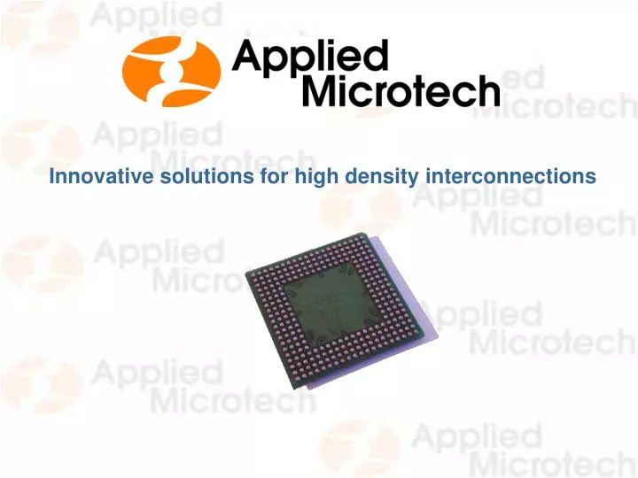
Innovative solutions for high density interconnections. Company Objective. To be the reference in ball soldering equipment through R&D and partnership development. Key activity : AMI or Alloy Micro Injection. A revolutionary process for area array package production.

E N D
Company Objective • To be the reference in ball soldering equipment through R&D and partnership development.
Key activity : AMI or Alloy Micro Injection A revolutionary process for area array package production To answer today’s cost needs and tomorrow ’s technological needs
Allows dramatic reduction in TCOO – up to 50% • Current technology uses • expensive balls which are • positioned through pick & place • Or stencil print process • Applied Microtech’s AMI • only requires inexpensive • alloy bars which are molten • to form the balls
AMI 700 PRODUCTION MODULE AMI - Alloy Micro Injection First commercialized module for Micro Injection production
Process Steps Current technology A.M.I. technology
Lower energy consumption Dramatic reduction in water consumption No flux or detergents Savings Necessary where water is scarce In line with IC manufacturer’s corporate policies Environmentally Friendly
Temperature profile Reflow oven
Temperature profile A.M.I process for leadless solder Component damage Process windows
Metal corrosion With leadless solder Inox 304
T.C.O.O comparison ( PBGA 276, 760 µm Ball diameter )
Looking to a bright future • Applied Microtech’s patented technology is set to be the reference for WLP bumping as well as wafer bumping. • 1st level of interconnect of substrates is also an ideal candidate for our technology.
R&D High density road map Alloy Micro Injection Pitch 0,15 Wafer Bumping 1st level substrate bumping 0,3 Wafer Level Packaging 0,5 CSP 0,8 BGA 1,0 Q2 2002 Q4 2002 Q2 2003 Q4 2003 Q2 2004
Thank you Questions & Answers