Download
1 / 18
180 likes | 315 Views
Effects of Device Aging on Microelectronics Radiation Response and Reliability. D. M. Fleetwood, M. P. Rodgers, L. Tsetseris, X. J. Zhou, I. Batyrev, S. Wang, R. D. Schrimpf, and S. T. Pantelides Vanderbilt University, Nashville, TN 37235 (dan.fleetwood@vanderbilt.edu)

E N D
Effects of Device Aging on MicroelectronicsRadiation Response and Reliability D. M. Fleetwood, M. P. Rodgers, L. Tsetseris, X. J. Zhou, I. Batyrev, S. Wang, R. D. Schrimpf, and S. T. Pantelides Vanderbilt University, Nashville, TN 37235 (dan.fleetwood@vanderbilt.edu) Work supported in part by AFOSR MURI and US Navy
Outline • Previous Work • Effects of burn-in, pre-irradiation temperature stress • Aging and baking effects on unpassivated capacitors • Aging effects on transistors • Parts stored in a non-hermetic environment • Parts stored hermetically sealed • Humidity testing • Density functional theory calculations • Hardness assurance implications
Effects of pre-irradiation elevated temperature stress Example of pre-rad temperature stress reducing oxide traps in field oxide Example of burn-in reducing interface traps in gate oxide M. R. Shaneyfelt, et al., IEEE Trans. Nucl. Sci. vol. 41, 2550 (1994) M. R. Shaneyfelt, et al., IEEE Trans. Nucl. Sci., vol. 43, 865, 1996.
1 0.6 Unbaked Unbaked baked 0.8 baked 1986 0.4 0.6 DNit (1012 cm-2) DNot (1012 cm-2) DNot (1012 cm-2) 0.4 0.2 0.2 0 0 0 200 400 600 800 1000 1200 0 200 400 600 800 1000 1200 Dose [krad(SiO2)] Dose [krad(SiO2)] Aging effects in unpassivated, Al gate capacitors tox = 33 nm; bias during rad = 5 V; bias during bake = 0 V A. P. Karmarkar, B. K. Choi, R. D. Schrimpf, and D. M. Fleetwood, IEEE Trans. Nucl. Sci., vol. 48, pp. 2158-2163, 2001.
Experimental Details: Aging Study • Fully processed and passivated poly-Si gate MOS transistors • 32 nm, stored non-hermetically • 60 nm, stored hermetically • 60 nm, stored non-hermetically • Parts from same lot well characterized in 1988 • 10-keV X-ray irradiation at dose rates of 100 and 850 rad(SiO2)/s for 60 and 32 nm, parts respectively • 6 V bias applied to all nMOS gates with all other pins held at ground, for rad + anneal • Midgap method of Winokur and McWhorter used to estimate ∆Vot and ∆Vit WINOKUR etal. 1987 • D. M. Fleetwood et al. IEEE TNS Vol. 35, No. 6, 1497, Dec. 1988
1988 Parts were packaged & hermetically sealed in 1987 Parts were irradiated to 500 krad(SiO2) Parts were delidded Data recorded throughout the postirradiation anneal. (room temperature) Parts were stored Parts were stored (not hermetically sealed) Parts were irradiated to 500 krad(SiO2) 3 of the 6 parts were baked @ 200C with all pins grounded prior to irradiation (PETS) 2005 Data recorded throughout the postirradiation anneal. (room temperature) 2 months after irradiation parts subjected to a high temperature anneal parts @ 100C Half of the parts were not baked Test Procedure: 32 nm, non-hermetically stored
32 nm devices, non-hermetic: ∆Vth 500 krad(SiO2) M. P. Rodgers, D. M. Fleetwood, R. D. Schrimpf, I. G. Batyrev, S. Wang, and S. T. Pantelides, IEEE Trans. Nucl. Sci. 52, 2642-2648 (2005).
32 nm devices, non-hermetic: ∆Vit 500 krad(SiO2) M. P. Rodgers, D. M. Fleetwood, R. D. Schrimpf, I. G. Batyrev, S. Wang, and S. T. Pantelides, IEEE Trans. Nucl. Sci. 52, 2642-2648 (2005).
32 nm devices, non-hermetic: ∆Vot 500 krad(SiO2) M. P. Rodgers, D. M. Fleetwood, R. D. Schrimpf, I. G. Batyrev, S. Wang, and S. T. Pantelides, IEEE Trans. Nucl. Sci. 52, 2642-2648 (2005).
Parts were packaged & hermetically sealed in 1987 Parts were delidded & irradiated to 100 krad(SiO2) 1988 Parts were stored Data recorded throughout the postirradiation anneal. (room temperature) Parts were irradiated to 100 krad(SiO2) Half of the parts were baked @ 200C with all pins grounded prior to irradiation (PETS) 2005 Data recorded throughout the postirradiation anneal. (room temperature) Parts were delidded 2 months after irradiation parts subjected to a high temperature anneal parts @ 100C Half of the parts were not baked Test Procedure: 60 nm, hermetically stored
60 nm devices, hermetic: ∆Vth 100 krad(SiO2) M. P. Rodgers, D. M. Fleetwood, R. D. Schrimpf, I. G. Batyrev, S. Wang, and S. T. Pantelides, IEEE Trans. Nucl. Sci. 52, 2642-2648 (2005).
32 nm devices, non-hermetic: ∆Vit 100 krad(SiO2) M. P. Rodgers, D. M. Fleetwood, R. D. Schrimpf, I. G. Batyrev, S. Wang, and S. T. Pantelides, IEEE Trans. Nucl. Sci. 52, 2642-2648 (2005).
32 nm devices, non-hermetic: ∆Vot 100 krad(SiO2) M. P. Rodgers, D. M. Fleetwood, R. D. Schrimpf, I. G. Batyrev, S. Wang, and S. T. Pantelides, IEEE Trans. Nucl. Sci. 52, 2642-2648 (2005).
60 nm devices: stored non-hermetically Dose: 100 krad(SiO2); 6V bias Similar enhancement in interface-trap buildup to 32 nm devices, stored non-hermetically
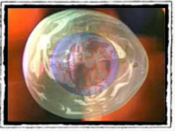
Source of extra hydrogen Left: Water complex consisting of two SiOH (silanol) groups and a broken ring [energy = +(0.3-0.7) eV] Right: Water complex consisting of two SiOH groups and no broken ring [energy = -0.3 eV]. Water that diffuses into SiO2 naturally dissociates, providing extra H+ to enhance interface-trap formation M. P. Rodgers, et al., IEEE Trans. Nucl. Sci. 52, 2642-2648 (2005).
Supporting evidence: humidity testing 130C at 85% Relative Humidity; 0 V Rad: 100k, 6V Anneal, 6V Enhancement due to increased interface-trap buildup during post-irradiation anneal
Irradiate to spec level 50 - 300 rad(Si)/s Electrical Test < 2 hr Biased Anneal @ T=25 C Pass ? No Electrical Test Yes Irradiate to 0.5x spec 50 - 300 rad(Si)/s Pass ? Yes Biased Anneal 168 hr @ 100 C No Reject Parts Electrical Test < 2 hr Pass ? Parts OK Reject Parts Yes No Implications for hardness assurance • 50% margin in irradiation not sufficient to describe aging-induced increase in for non-hermetically stored devices • Exposing parts to PETS does not simulate the aging effects observed in these parts • Additional margins required in hardness assurance testing for parts susceptible to enhanced interface-trap buildup during aging • Combining the aging and PETS effects shown may explain previous complications in low-dose-rate response of MOS and bipolar devices
Conclusions • Radiation response of MOS devices can change significantly with aging time after processing and/or packaging. • Effects are most significant for interface trap buildup during post-irradiation annealing. • Theory, as supported by the results of humidity tests, suggests that the increase in degradation is associated with H2O or other H-containing complexes. • Non-hermetic environments are especially challenging. • How hermetic is hermetic enough? • Some effects seen even for hermetic environments, likely due to on-chip sources of hydrogen. • Extra margins required in lot acceptance testing for sensitive devices/environments.