Download
1 / 19
210 likes | 387 Views
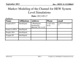
Development of front-end electronics for Silicon Photo-Multipliers F. Corsi, A. Dragone, M. Foresta, C. Marzocca, G. Matarrese, A. Perrotta INFN DASiPM Collaboration DEE - Politecnico di Bari and INFN Bari Section, Italy. Main activities.

E N D
Development of front-end electronics for Silicon Photo-Multipliers F. Corsi, A. Dragone, M. Foresta, C. Marzocca, G. Matarrese, A. Perrotta INFN DASiPM Collaboration DEE - Politecnico di Bari and INFN Bari Section, Italy
Main activities • Accurate modelling of the SiPM for reliable simulations at circuit level. • Development of an extraction procedure for the parameters involved in the model. • Validation of the model accuracy. • Comparison of different front-end approaches. • Preliminary results of the first version of front-end based on a current buffer .
Electrical model of a SiPM • Rq: quenching resistor • (hundreds of kW) • Cd: photodiode capacitance • (few tens of fF) • Cq: parasitic capacitance in parallel to Rq (smaller than Cd) • IAV: current source modelling the total charge delivered by a microcell during the avalanche Cg : parasitic capacitance due to the routing of the bias voltage to the N microcells, realized with a metal grid. Example: metal-substrate unit area capacitance 0.03 fF/mm2 metal grid = 35% of the total detector area = 1mm2 Avalanche time constants much faster than those introduced by the circuit: IAV can be approximated as a short pulse containing the total amount of charge delivered by the firing microcell Q=DV(Cd+Cq), with DV=VBIAS-VBR Cg 10pF, without considering the fringe parasitics
Extraction of Rq Forward characteristic of the SiPM, region in which DV/DI is almost constant and equal to Rq/N. _____ Measured characteristic _____ Least square linear fit Forward characteristic of a SiPM produced by ITC-irst. Slope = 1.59 mS Rq/N = 629 W N = 625 Rq = 393 kW
Extraction of Vbr and Cd+Cq * Measured points __ Least square linear fit Q [C] Vbias [V] Example of a single dark count pulse for the ITC-irst SiPM (obtained by reading the pulse with a 50W resistor and using a 140 gain, fast voltage amplifier) Charge contained in a single dark count pulse vs. bias voltage Charge associated to a single dark count pulse as a function of the bias voltage: Q=(Cd+Cq)(Vbias-Vbr) Cd+Cq and, by extrapolation, Vbr
Extraction of Cd, Cq and Cg YM [mS] CM [pF] Vbias [V] Vbias [V] Rqtot Cqtot YM CM Cg Cdtot CV plotter measurements near the breakdown voltage: YM and CM According to the SiPM model, YM and CM are expressed in terms of Cdtot=NCd, Cqtot=NCq, Rqtot=Rq/N and the frequency w of the signal used by the CV plotter. CV plotter measurement results for the same device from ITC-irst. The signal frequency is 1 MHz. Cd,Cq Cg
Results of the extraction procedure • Extraction procedure applied to two SiPM detectors from different manufacturers. • The table summarizes the main features of the devices and the results obtained. • Good agreement with the expected parameter values estimated on the basis of technological and geometrical parameters.
Vbias Vbias Vbias CF SiPM SiPM SiPM - + kIS=IOUT IS RS RS - + VOUT VOUT The charge Q delivered by the detector is collected on CF If the maximum DVOUT is 3V and Q is 50pC (about 300 SiPM microcells), CF must be 16.7pF Perspective limitations in dynamic range and die area with low voltage, deep submicron technologies Front-end electronics: different approaches Charge sensitive amplifier Voltage amplifier Current buffer A I-V conversion is realized by means of RS The valueofRS affects the gain and the signal waveform VOUT must be integrated to extract the charge information: thus a further V-I conversion is needed RS is the (small) input impedance of the current buffer The output current can be easily reproduced (by means of current mirrors) and further processed (e.g. integrated) The circuit is inherently fast The current mode of operation enhances the dynamic range, since it does not suffer from voltage limitations due to deep submicron implementation
SiPM + front-end behaviour IIN + Rq (N-1)Cq Cg Rq/(N-1) RS VIN - Cd (N-1)Cd IAV IIN + Cg Cd Cq Ceq IAV Rq VIN Iq RS - Iq The load effects, the grid parasitic capacitance and the value of Rs are key factors in the determination of the resulting waveform of VIN and IIN A qualitative study of the circuit can be carried out with reference to the simplified schematic depicted below. The two circuits give very similar results, provided that Rs is much lower than Rqtot=NRq Cq A) SiPM coupled to an amplifier with input impedance Rs B) Simplified circuit
SiPM + front-end behaviour Rs=75W VIN Rs=50W Rs=20W Time Responses of the circuits A) and B) to a single dark pulse (160fC) for three different values of Rs and typical parameter values • The simulations show that the peak of VIN is almost independent of Rs. • In fact, a constant fraction QIN of the charge Q delivered during the avalanche (considered very fast with respect to the time constants of the circuit) is instantly collected on Ctot=Cg+Ceq. • The simplified circuit has two time constants: • tIN= Rs Ctot • tr=Rq(Cd+Cq) • Decreasing Rs, the time constant tIN decreases, the current in Rs increases and the collection of the charge is slightly faster, as shown by the simulations. _____ Circuit A) _____ Circuit B)
Bandwidth of the amplifier _____ BW=500MHz _____ BW=100MHz VOUT Rs=20W Time _____ BW=500MHz _____ BW=100MHz VOUT Rs=75W Time Amplifier output voltage for a single dark pulse: same gain and different bandwidth • The simulations show the output of a voltage amplifier for two different Rs and bandwidths. • The bandwidth of the amplifier directly affects the rise time of the waveform, independently of the value of RS. • The peak amplitude of the waveform is strongly dependent on the amplifier bandwidth, especially for low values of RS. In fact, in this case tIN can be very fast compared to the dominant time constant of the amplifier, which is unable to adequately reproduce the input signal. • The time needed to collect the charge is just slightly influenced by the amplifier bandwidth. • The same conclusions are valid also for the waveform of the output current obtained with a current buffer
Experimental validation of the model Two different amplifiers have been used to read-out the ITC-irst SiPM a) Transimpedance amplifier BW=80MHz Rs=110W Gain=2.7kW b) Voltage amplifier BW=360MHz Rs=50W Gain=140 • The model extracted according to the procedure described above has been used in the SPICE simulations • The fitting between simulations and measurements is quite good
Current buffer: two alternative solutions Buffer2 Buffer1 • CMOS 0.35um standard technology • Feedback applied to reduce input resistance and increase bandwidth
Integrated current buffer: two alternative solutions • Buffer1 • simple structure • more bandwidth (≈ 300 MHz) • limited dynamic range • Buffer2 • more complex • a little slower (BW 250 MHz) • extended dynamic range
Experimental setup Current Buffer Voltage Amplifier 50Ω BNC Pulse Generator BlueLed SiPM 100Ω Iout Vbias Experimental setup Test board V Input waveform 8ns 7V t 4.5ns 4.5ns
Preliminary results: output waveforms Measure Buffer2 Buffer1 • The test board is the bottleneck for the BW of the whole system • The total no. of photons is always the same in all measurements • The standard deviation of the current peak corresponds to about 1/2 micro-cell
Preliminary results: linearity Measure • The first solution exhibits limited dynamic range and gain, as expected
Future work Measure • More measurements on the current buffers with known ligth source • Definition of the architecture (shaper? current peak detector? on chip ADC?) • 9 channel test chip • Migration to another technology (for instance 0.18um) • Final task: 64 channel ASIC