Download
1 / 23
230 likes | 462 Views
Measurement of SEU on the Module Controller Chip of the ATLAS Pixel Detector. G.Gagliardi – INFN and University – Genova On behalf of the ATLAS Pixel Collaboration. ATLAS Pixel Detector. The ATLAS detector is a multipurpose detector to be installed in the Large Hadron Collider at CERN

E N D
Measurement of SEU on the Module Controller Chip of the ATLAS Pixel Detector G.Gagliardi – INFN and University – Genova On behalf of the ATLAS Pixel Collaboration
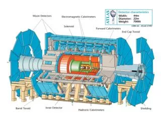
ATLAS Pixel Detector • The ATLAS detector is a multipurpose detector to be installed in the Large Hadron Collider at CERN • Inner tracking is performed by a combination of silicon and gaseous detector. The ATLAS Pixel Detector is the innermost component of the tracking system and provides critical tracking information for pattern recognition near the LHC collision point. • The innermost pixel layer (B-Layer) is located at ~50 mm from the interaction point while the outermost layer is at ~120 mm from the interaction point. • The expected integrated dose in 10 year of LHC operation for the middle layer of the Pixel Detector is ~50 Mrad, while for the B-Layer the expected dose is ~5 times higher. The B-layer is supposed to be replaced after a few year data taking • The expected SEE (Single Event Effects) rate (which includes effect from charged hadrons and neutrons with energy greater than 20 MeV) is ~ 3 E14 particle/cm2/y for the B-Layer, while is in the range of 0.5 ÷ 0.9 E14 for the other layers.
Pixel Detector Module • The ATLAS Pixel Detector is composed of ~2000 modular units, identical for all the detector layers. • The readout of the ~ 46.000 channels of a Pixel Module is performed by 16 Front End (FE) chips bump-bonded to the sensor • An additional read-out electronic, the Module Controller Chip (MCC), handles the event building at module level, as well as the 16 FE chips configuration and control. • Input/output of the module is limited to three optical fibers, one for command and two for data. The data readout can be performed with bandwidth ranging from 40 Mb/s (one data link used) up to 160 Mb/s (two data link at 80 Mb/s used)
Module Controller Chip Architecture • System startup and configuration. Decode configuration data and command signals from module command link and store configuration data into a register bank. • Trigger, Timing and Control: the MCC has to provide LV1 triggers to all FE chips and keep event synchronization. • Receive serial data from 16 FE chips, accumulate data in local FIFO's. • Event building: complete module events are reconstructed with some data compression and assigned to the correct LV1 number stored in the Pending LV1 FIFO. • Error handling: FIFO overflows, misalignment of data from FE chips with BCID information, disable defective or noisy FE chips,… Error flags are stored into the register bank.
The MCC-I1 • The MCC-I1 is a 0.25 micron CMOS digital chip • It has been synthesized from a full HDL (Verilog) description with Synopsys using the standard cell library developed at CERN and maintained by RAL. • The Pending LV1 FIFO (Pending Event FIFO, PEF in the following), the register bank and the state machines makes use of the DFF_SR_SC (Standard Cell Flip-Flop, SC_FF in the following) cell of the library. • The 16 receiver FIFOs are provided using a full custom dual port RAM developed at CERN (Full Custom Memory Cell, FC_MC in the following) • Die size is 6.38 x 3.98 µm2. The total number of Standard Cell used is 16K, the number of transistors is 660K. The number of DFF_SR_SC used as configuration data memory element or in the state machines is ~ 2K Receiver FIFO Standard Cell with embedded Register Bank and PEF
Meauserement of SEU in the MCC • Seven MCC-I1 were irradiated from July, 1st to July, 10th 2002 at CERN PS with a 24 GeV proton beam in order to check the chip radiation hardness and the SEU rate. • All 7 chips were tested as good before the irradiation. • The chip were mounted on single-boards and put in a removable shuttle. The temperature on the board was monitored and kept at ~ 0 C°. • Use of dedicated electronics to command and read-out the 7 chip. • Three chips supplied with 1.8 V DVDD and four with 2.2 V DVDD. Although the standard cell library is qualified at 2.5 V, the MCC-I1 passed full functionality lab tests at 70 MHz input clock and 1.6 V DVDD.
MCC-I1 Irradiation Beam Line
MCC-I1 Irradiation • The real time integrated dose was 3.22 1015 proton/cm2. • The actual dose on the MCC-I1 was monitored by Al foil placed behind each board. The activation measurements were consistent with each other. The mean measured value is 2.66 1015 proton/cm2. • Assuming the conversion factor of 29 10-15 Mrad/(proton/cm2) this leads to a conservative value for the integrated dose of ~ 71 Mrad. • All the seven chips under test were fully functional up to the end of the irradiation: neither sign of dead lock has been seen or need of a pin reset have been necessary to restart the chip. The command decoder state machines are designed to return to the idle state from any state, thus being protected against bit flip.
MCC-I2 Irradiation – SEU test • The SEU test detected the modification of data stored into standard cell flip-flops (SC FF) and into the full custom memory cell of the Receiver FIFOs (FC MC) induced by the proton flux. • 304 SC FF of the MCC-I1 were tested • The register tested were the Warning Front End register (WFE), the Warning MCC register (WMCC), the Front-End ENable register (FEEN) and the Pending Event FIFO (PEF) • 53760 FC MC were tested • Before each PS particle spill, configuration data was written. After the spill data was read back and compared with written data in order to understand static bit flip probability. • At each spill the proton flux was measured allowing the measurement of the SEU cross section • Control runs were done performing the SEU tests with the shuttle put in PARK position (far from the beam). No SEU’s were detected in those control runs.
SEU effects • The SEU effect is detected as a flipping of the data stored into the SC FF and FC MC. spill 245 - mcc 5 - ok TRUE loc good bad 0 ffff ffff 1 eeee eeee 2 dddd fddd * 3 cccc cccc 4 bbbb bbbb 5 aaaa aaaa 6 9999 9d99 * 7 8888 8888 8 7777 7777 9 6666 6666 10 5555 5555 11 4444 4444 12 3333 3333 13 2222 22a2 * 14 1111 1111 15 0 800 * SEU (one star per bit flip) PEF location with SEU Expected values Read values
SEU effects – Receiver FIFO • The SEU effect in the Receiver FIFO FC MC is detected as a change the data stored into the Receiver FIFO locations by one or a few bits. . . . 107 50a14 50a14 108 4c993 4c993 109 48912 48911 ** 110 44891 44891 111 40810 40810 112 3c78f 3c78f 113 3870e 3870e 114 3468d 3468d 115 3060c 3860c * 116 2c58b 2c58b 117 2850a 2850a 118 24489 a4489 * 119 20408 20408 120 1c387 1c387 121 18306 18306 . . . • . . . • 50 dd932 dd932 • 51 dd9b3 dd9b3 • 52 dda34 dda34 • 53 ddab5 ddab5 • 54 ddb36 ddb36 • 55 ddbb7 ddbb7 • 56 ddc38 ddc38 • 57 ddcb9 ddcb9 • 58 ddd3a ddd3a • 59 dddbb ddcbb * • 60 dde3c dde3c • 61 ddebd ddebd • 62 ddf3e d5f3e * • ddfbf ddfbf • . . .
Global SEU effects • There are also SEUs that have a global impact on the data stored. This is because is the state machine flip-flip to flip, rather than the memory one. • The examination of the data read back from the register bank leads to the individuation of definite categories of global SEU effects. • This particular effect is understood as a SEU in the counter that controls the PEF write pointer. sp 638 - mcc 5 - ok FALSE loc good bad 0 0 0 1 1111 1111 2 2222 2222 3 3333 3333 4 4444 4444 5 5555 5555 6 6666 6666 7 7777 7777 8 8888 8888 9 9999 8888 **** 10 aaaa 8888 **** 11 bbbb 8888 ******** 12 cccc 8888 **** 13 dddd 8888 ******** 14 eeee 8888 ******** 15 ffff 8888 ************ spill 469 - mcc 1 - ok FALSE loc good bad 0 ffff ffff 1 eeee eeee 2 dddd dddd 3 cccc cccc 4 bbbb bbbb 5 aaaa aaaa 6 9999 9999 7 8888 8888 8 7777 7777 9 6666 6666 10 5555 5555 11 4444 4444 12 3333 3333 13 2222 3333 **** 14 1111 3333 **** 15 0 3333 ********
Global SEU effects – Receiver FIFO • We observe global SEU effects in the Receiver FIFOs. • spill 833 - mcc 7 • fifo 13 • loc good bad • isok FALSE • 0 1fffff 0 ********************* • 1 1fbf7e 1fbf7e • 2 1f7efd 1f7edd * • 3 1f3e7c 1f3e7c • 4 1efdfb 1efdfb • 5 1ebd7a 1ebd7a • 6 1e7cf9 1e7cf9 • 7 1e3c78 1e3c78 • 8 1dfbf7 1dfbf7 • 9 1dbb76 1dbb76 • 10 1d7af5 1d7af5 • 11 1d3a74 1d3a74 • 1cf9f3 1cf9f3 • . . . spill 845 - mcc 1 fifo 7 loc good bad isok FALSE 0 1fffff 4000 ******************** 1 1fbf7e 1faf7e * 2 1f7efd 1f7efd 3 1f3e7c 1f3e7c 4 1efdfb 1efdfb 5 1ebd7a 1e3d7a * 6 1e7cf9 1e7cf9 7 1e3c78 1e3c78 . . .
SEU x-section measure • A measure of the SEU x-section for the SC FF and FC MC has been done using the bit flip rate in the selected sample and the radiation dose recorded during the spills. • FC MC SEU x-section is twice as big than SC FF SEU x-section. • There is no definite increase of the SEU x-section with the integrated dose. • The chips supplied with 1.8 V DVDD have a SEU x-section for both FC MC and SC FF larger than the ones for 2.2 V DVDD chips. The 1.8V/2.2V SEU x-section ratio is ~ 2 for the SC FF and ~ 1.8 for the FC MC.
SC FF SEU x-section • This plot shows also the SEU x-section for two run with the clock on.
SEU measured x-section and the Pixel Detector • Using the standard ATLAS irradiation figure for the B-Layer – 3x10¹⁴ proton/cm2 in one year (107 s) of data taking - it is possible to crude estimate the effect of the measured SEU x-section for the Pixel Detector. • Two effects are considered as benchmarks: the flipping of one of the memory cell of the hit FIFO that induce a synchronization lost and the flipping of one of the ~2000 FF of the state machines in the MCC-I1. • In the pessimistic picture – i.e. data corruption and stop of standard behavior for the MCC-I1 every SC FF SEU flip, with one periodical reset every ~ 100 s and the chip operated at DVDD 2.2 V – the fraction of the data taking time when module data are corrupted is ~ 6%. • The inefficiency can be significantly reduced by ROD inspection of data and automatic recover. FC MC flip inducing loss of synchronism MCC-I1@2.2V ~3280 s (for the whole B-Layer ~11 s) MCC-I1@1.8V ~1860 s (for the whole B-Layer ~6 s) SC FF flip MCC-I1@2.2V ~1620 s (for the whole B-Layer ~6 s) MCC_I1@1.8V ~780 s (for the whole B-Layer ~3 s)
The 0->1/1->0 ratio • The ratio of bit flip from “0” to “1” and the opposite has been measured as well • The writing phase of the SEU test loaded the SC FF and the FC MC with known values. Particular care was taken in balancing the number of memory bits set to 1 and to 0, in such a way to insure a uniform exposure for each internal structure during the irradiation. • The ratio do not depends on the DVDD value
SEU FIFO spatial correlation • Looking at the Receiver FIFO locations with two bit flips there is evidence for the correlated production of FC MC bit flip in pairs. Only nearest neighbor double flip production is enhanced, i.e. there is no or very little correlation between FC MC bit flip production for which the spatial distance in the chip is greater than the size of the memory cell (in our case 5.60 mm). • The double bit flip excess is related to the energy released by a particle in the two FC MC. It is possible to measure the SEU FC MC nearest neighbor double bit flip in the Receiver FIFO locations. • The overall fraction of FC MC SEU nearest neighbor double flip is small, so that the effect on the FC MC SEU x-section is negligible (ranging from 0.3 to 0.5 % of the FC MC SEU x-section)
SEU double flip spatial correlation Proton flux 1.3 1011/spill Integrated proton flux 1.35 1014
Looking forward… • A new version of the Module Controller Chip – MCC-I2 – has been realized • A protection against the SEU has been provided in the new chip by triplicating most of the states machines • The whole Command Decoder has been triplicated with a majority voting circuit on all outputs. • All Control bits of the Register Bank have been triplicated • The Event Builder Control FSM has been triplicated • All control signals generated by the Receiver block and all counters dealing with writing data in the FIFO have been triplicated. • No automatic error correction has been built-in, so that one still has to make sure to rewrite the correct values as soon as possible in order to avoid errors. • The FIFO now has a SEU proof encoding in data written to it • Those changes should reduce the impact of SEU on the module operation • Intelligence in the upstream DAQ electronics is in any case foreseen • The new chip is back from foundry • After the lab tests the chip is foreseen to be irradiated during this summer at PS