Download
1 / 21
210 likes | 295 Views
Read-Out Driver for ATLAS Silicon Detectors. Atlas Wisconsin/LBNL Group March 21 st 2007. ATLAS Pixel B-Layer Upgrade Workshop. Silicon Read Out Driver (SiROD). Silicon RevE(F) SiROD. Clock Distribution. Slave DSPs. Router FPGA. VME Interface. 9U VME. Controller FPGA. Event

E N D
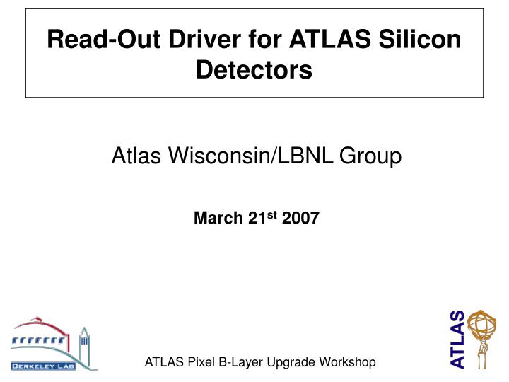
Read-Out Driver for ATLAS Silicon Detectors Atlas Wisconsin/LBNL Group March 21st 2007 ATLAS Pixel B-Layer Upgrade Workshop
Silicon RevE(F) SiROD Clock Distribution Slave DSPs Router FPGA VME Interface 9U VME Controller FPGA Event Fragment Builder FPGA Master DSP Formatter FPGAs
ROD Overview (1) • FE Module Interface: • 96 FE Data input connections available • 48 FE Command output connection available • 2048x32 Data FIFO for each Module (32 total) • Pixel B-Layer: 6-7 modules • 12-14 80MHz input data links • 6- 7 40MHz output command links • Pixel Barrel L2: 26 modules • 26 40MHz input data links • 26 40MHz output command links • Pixel Disks: 13 modules (26 ROD channels) • 13 80MHz input data links • 13 40MHz output command links
ROD Overview (2) • Diagnostic components included for stand alone testing • Maintain data throughput at 100kHz trigger rate • Flexible calibration processes • MDSP Control • ROD Controller FPGA Control • TIM Control
ROD Control/VME Path Back Of Crate (BOC) VME Slave FPGA Configuration Controller ROD BUSY Histogram 16Mb Flash Memory Master DSP TI 320C6201 160MHz DIAGNOSTIC FIFOs ROUTER FPGA 32 MB SDRAM FORMATTER FPGA 8x ROD CONTROLLER FPGA EFB FPGA BOOT ROM 512KB VME Bandwidth: ~8MB/s MDSP~4MB/s SDSP~22MB/s VME Slave A32/D32 CNFG DATA to All FPGAs VME Bus ROD BUSY RESET D16 RODBus D16 DSP FARM TI 320C6713 220MHz 256MB SDRAM 4x D32 All DSPs: 16 bit Host Port Interface MDSP EMIF
ROD CONTROLLER FPGA: Control Functions MDSP Serial Port Interface Control & Status Registers Reset Command Interface DSP Interrupt Interface Diagnostic FIFO Interface RCF RODBus Interface (FPGAs, DSP Farm) To VME/PRM FPGA To MDSP SP0/SP1 ports MDSP Interrupts SDSP Interrupts INPUT FIFO (32K x 96) EVENTMEM FIFO (16K x 48) MDSP EMIF Data (32) RODBus Data (16) MDSP EMIF Address RODBus Address MDSP EMIF Control RODBus Control
MDSP: Primitive List State Machine • Primitive List execution: Host-to-MDSP and MDSP-to-SDSP Primitive List Execution IDLE inList Bit Cleared By Host? YES NO NO ACKNOWLEDGE List Inserted? Resume? NO YES Abort? YES PAUSED EXECUTING (one primitive per Iteration) NO YES PREPARE REPLY YES Pause? YES NO NO Finished or Abort?
Text Buffer State Machine • Text Buffer reply: MDSP-to-Host and SDSP-to-MDSP • Error, Info, Diagnostic and Transfer (MDSP is a way-station for SDSP text buffers) Text Buffer Transmission IDLE YES NO Buffer Read? Buffer Occupied? YES NO FROZEN WAITING YES NO Read Request?
SiROD DATA PATH S-Link BOC TIM BOC INPUT FIFO 32K Deep FORMATTER FPGA FORMATTER FPGA FORMATTER FPGA FORMATTER FPGA FORMATTER FPGA FORMATTER FPGA FORMATTER FPGA FORMATTER FPGA DSP FARM TI 320C6713 220MHz 256MB SDRAM 4x EFB FPGA XC2S400-6FG676 ROUTER FPGA XC2S400-6FG456 EVENTFIFOs 216Kx48 ROD CONTROLLER FPGA XC2S600-6FG676 XC2S600-6FG456 Can sustain 100KHz Trigger Rate into S-Link Event Fragments Xoff A Xoff B Xoff EVENT ID TTC READOUT ROD BUSY MDSP SP FE CMD (48)
ROD CONTROLLER FPGA: Real Time Functions Trigger Processor & Counter FE Command Processor & Mask Event Processor Dynamic MasksMode BitsEvent ID Data Trigger Type Diagnostics Generator Control & Status Registers FE Event Counter Internal Scan Processor RCF RODBus Interface MDSP Ser Port 0 MDSP Ser Port 1 FE CMD (48) TTC L1 Trigger TTC EVT EFB EVT (16) FMT MB (12) FMT Trailer Detect MDSP EMIF Data (32) RODBus Data (16) MDSP EMIF Address RODBus Address MDSP EMIF Control RODBus Control
PIXEL FORMATTER FPGA (8x) Read Out Controller Link Input MUX & Half Clock Counters Control & Status Registers (32) Link FIFO 2048 x 32 Link Decoder: 40/80/160MHz Link FIFO 2048 x 32 Link Decoder: 40/80MHz Link FIFO 2048 x 32 Link Decoder: 40MHz Link Decoder: 40MHz Link FIFO 2048 x 32 RODBus Interface Trailer Detect ModeBits FIFO 512x24 DATA OUT (40) IN0 IN1 IN2 IN3 IN4 IN5 IN6 IN7 IN8 IN9 IN10 IN11 ROD BUSY HT LIMIT TOKEN FMT ID TRAILER (12) FMT Type RODBus Data (16) RODBus Address FMT MB (12) RODBus Control
EVENT FRAGMENT BUILDER FPGA EventMemB FIFO 16Kx48 EventMemA FIFO 16Kx48 FIFO Controller Purpose: Collect Formatter output, check L1 and BC IDs, count errors, generate Event Header & Trailer Engine 0 Halt Output Formatter Num. (2 bits) Link Num. (6 bits) Link Num. (4 bits) Time-out Error To/From Formatter Output FIFO Data (43) Data (32 bits) L1ID Error INC/DEC L1ID Format & Count Error Check L1/BC ID Check Time Out BCID Error Data (32 bits) Data Valid Xoff Error Summary Word Event Data & Trigger Type To/From Router Header and Trailer Data (32) Header/Trailer Generator To/From Controller L1 & BC IDs Dynamic Mask EventMemC Error Summary Word Data Valid Data (32 bits) BCID Error Time Out INC/DEC L1ID Format & Count L1/BC ID Check Error Check L1ID Error Data (32 bits) To/From Formatter Time-out Error Link Num. (4 bits) Link Num. (6 bits) Formatter Num. (2 bits) Halt Output Engine 1
ROD Router (FPGA) & Slave DSPs Purpose: Route formatted data to Level-2 and/or Slave DSPs (histogram) Halt Output XOn / XOff S-Link Dsp Halt Output S-Link Data Event Header and Trailer Data (32b) S-LINK To/From ROS Read, format and direct the event data To/From Event Fragment Builder Output FIFO (43b) Data Valid Error Format Data 2 Traps 2 Traps 2 Traps 2 Traps Event Type: ATLAS, ROD or TIM Event Type: ATLAS, ROD or TIM Event Type: ATLAS, ROD or TIM Event Type: ATLAS, ROD or TIM DMA Transfer Engine DMA Transfer Engine DMA Transfer Engine DMA Transfer Engine 1024 32-bit FIFO 1024 32-bit FIFO 1024 32-bit FIFO 1024 32-bit FIFO SDSP 2 SDSP 0 SDSP 3 SDSP 1 Texas Instruments 6713 floating point DSPs running at 220 MHz for monitoring and calibration histogramming
The Silicon Read-Out Driver (ROD) • Primary purpose: Module configuration, Trigger propagation, Data formatting • A hybrid of FPGAs and DSPs • The Master DSP (MDSP) has ROD and BOC registers connected to one of its EMIFs (External Memory InterFace) Configuration & Triggers Event Fragment Builder Formatters Event Data Backpressure / Halt Output Router & Slave DSPs MODULE BOC (Back Of Crate) S-Link Controller & Master DSP ROD ROS (Read Out Subsystem) To Event-Builder and Level-2 SBC TIM (Single Board Computer) (TIming Module) Calibration Histograms • Secondary purpose: Calibrations / Monitoring • FPGAs for time-critical functions (Event Data Path) • DSPs for configuration, ROD control, calibrations and monitoring
Pixel Calibration Scans • A couple of common Pixel Scans: • Threshold (on chip charge-injection for each individual pixel; scan the number of hits for each injected charge to obtain the discriminator threshold) • Noise (a threshold scan without charge injection to measure noise) Threshold Scan result shown for a single Pixel Module Threshold for each pixel (note the 16 FE ICs)
SCT Calibration Scans • Some of the commonly run SCT Calibration Scans: • Rx Threshold Test (optimize the Rx threshold value in the BOC data-receiver chip) • NMask Test (demonstrate that the chip mask register functions properly) • Pipeline Test (scan the chip pipeline for defects; stuck on or off) • Full Bypass Test (does the chip bypass feature function properly) • Noise Occupancy Test (a threshold scan without charge injection to measure noise) • Synchronous Trigger Noise Test (triggers distributed synchronously across the system) N-Mask Scan result shown for a single SCT Module
ROD use during detector production / assembly • Calibration scans have been routinely used during module production • Verify module functionality before and after mounting or transport • Classification of modules • Rank by the number of defects; only mount and install the very best • This phase also gave feedback to ROD developers (and still continues to!) • A few DSP software and FPGA Firmware problems have been uncovered this way • Some unique bugs appeared when stressing the ROD with a full complement of modules
Cosmics Data-Taking A total of 504 SCT Modules into 12 RODs were used during the combined cosmics data-taking run • TRT/SCT combined run in May 2006 • ROD performed well; successfully collected more than 400k events • Useful DAQ/Detector shake-down, data for efficiency and alignment studies • On-ROD Histogramming used for timing • in the SCT during cosmics running • (i.e., delay the signal by the correct amount) Scintillator SCT Noise Number of coincident hits on top and bottom strips Transmission Delay (bunch-crossings) Scintillator Transition Radiation Tracker (TRT) 20 cm of concrete Scintillator
SCT RODs in USA-15 • Production RODs in their final location for ATLAS running