Download
1 / 21
210 likes | 343 Views
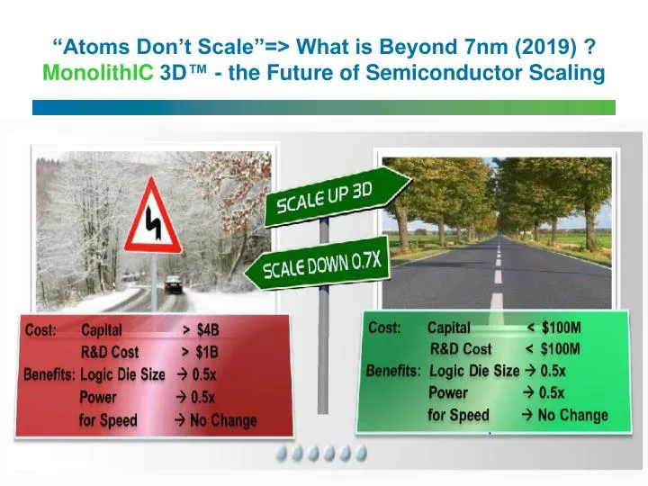
“Atoms Don’t Scale”=> What is Beyond 7nm (2019) ? MonolithIC 3D™ - the Future of Semiconductor Scaling. Intel, Steve Punta Oct 2012: Beyond 7nm ??? http://www.intel.com/content/dam/www/public/emea/eu/en/documents/eric/day2-steve-putna.pdf.

E N D
“Atoms Don’t Scale”=> What is Beyond 7nm (2019) ?MonolithIC 3D™ - the Future of Semiconductor Scaling
Intel, Steve Punta Oct 2012: Beyond 7nm ??? http://www.intel.com/content/dam/www/public/emea/eu/en/documents/eric/day2-steve-putna.pdf
EDA at the End of Moore’s Law*Bob Colwell, Director MTO, DARPA *CRA/CCC & ACM SIGDA, Pittsburgh, March 2013
The end of Moore's Law – The End of Dimensional Scaling Mike Mayberry, VP Technology and Manufacturing GroupIntel (5/2013) .. has looked down the highway of conventional silicon development and reckons things become foggy beyond about the 7-nm node < http://www.eetimes.com/electronics-news/4414897/More-varied-research-needed-says-Intel> The end of Moore's Law is on the horizon, says AMD (4/2013) Gustafson, chief graphics product architect at AMD, claimed "You can see how Moore's law is slowing down” http://www.zdnet.com/amd-sees-the-era-of-moores-law-coming-to-a-close-7000013413/ William Dally Nvidia’s vice president of R&D & chief scientist (3/2013) “Chip stacking is increasingly seen as an alternative to moving to the next semiconductor node at a time when process technology is providing less bang for the buck” http://www.eetimes.com/electronics-news/4410792/Nvidia-R-D-chief-sketches-road-to-chip-stacks Broadcom CTO Henry Samueli says (5/2013) “Broadcom is starting to prepare customers for the end of CMOS scaling in the next 15 years, and it is working out plans for 3-D chip stacks.” <http://www.eetimes.com/electronics-news/4415006/Broadcom--Time-to-prepare-for-the-end-of-Moore-s-Law>
The Current 2D-IC is Facing Escalating Challenges - I • On-chip interconnect is • Dominating device power consumption • Dominating device performance • Penalizing device size and cost
Connectivity Consumes 70-80% of Total Power @ 22nmRepeaters Consume Exponentially More Power and Area At 22nm, on-chip connectivity consumes 70-80% of total power Repeater count increases exponentially At 45nm, repeaters are > 50% of total leakage Source: IBM POWER processors R. Puri, et al., SRC Interconnect Forum, 2006 MonolithIC 3D Inc. Patents Pending
The Current 2D-IC is Facing Escalating Challenges - II Lithography is Dominating Fab cost Dominating device cost and diminishing scaling’s benefits Dominating device yield Dominating IC development costs
“Net: neither per wafer nor per gate showing historical cost reduction trends”
THE SOLUTION: 3D IC 10 MonolithIC 3D Inc. Patents Pending
Toshiba, Samsung, Intel..– NAND Vendors are already Adopting Monolithic 3D *2011 Symposium on VLSI Technology Digest of Technical Papers Jungdal Choi and Kwang Soo Seol Semiconductor R&D Center, Samsung Electronics Co., Ltd.
Conclusions: Dimensional Scaling (“Moore’s Law”) is already exhibiting diminishing returns The road map beyond 2017 (7nm) is unclear While the research community is working on many interesting new technologies (see below), none of them seem mature enough to replace silicon for 2019 - Carbon nanotube - Indium gallium arsenide - Graphene - Spintronics - Nanowire - Molecular computing - Photonics - Quantum computing 3D IC is considered, by all, as the near term solution, and Monolithic 3DIC is well positioned to be so, as it uses the existing infrastructure! It is safe to state that Monolithic 3D is the only alternative that could be ready for high volume in 2019 !!
Very Low Risk • The Technology is already developed • The base burn-rate is very low • >90 Patents filed • 34 Fundamental patents allowed (32 Issued) as of today • Full exclusivity on the monolithic 3D IC market • Full exclusivity on ‘wafer scale integration’ • Many other high value patents
Thin Layer Transfer Technology (“Smart-Cut”) The Technology Behind SOI * p- Si Oxide Oxide Oxide Oxide Cleave using 400oC anneal or mechanical force Hydrogen implant of top layer Flip top layer and bond to bottom layer Oxide p- Si Donor Wafer Oxide H+ < 100nm H+ p- Si Oxide Base Wafer Similar process (bulk-to-bulk) used for manufacturing all SOI wafers today Smart-Cut is a register trade mark of Soitec
The Top Layer has a High Temperature >1000C) without Heating the Bottom Layers (<400°C)!!! } >1000°C } <400°C
Innovation Enabling ‘Wafer Scale Integration’ – 99.99% Yield with 3D Redundancy Gene Amdahl -“Wafer scale integration will only work with 99.99% yield, which won’t happen for 100 years” (Source: Wikipedia) • Swap at logic cone granularity • Negligible design, or power penalty • Redundant 1 above, no performance penalty • Server-Farm in a Box • Watson in a Smart Phone • …
Monolithic 3D Provides an Attractive Path to… 3D-CMOS: Monolithic 3D Logic Technology 3D-FPGA: Monolithic 3D Programmable Logic 3D-GateArray: Monolithic 3D Gate Array 3D-Repair: Yield recovery for high-density chips 3D-DRAM: Monolithic 3D DRAM 3D-RRAM: Monolithic 3D RRAM 3D-Flash: Monolithic 3D Flash Memory 3D-Imagers: Monolithic 3D Image Sensor 3D-MicroDisplay: Monolithic 3D Display 3D-LED: Monolithic 3D LED Monolithic 3D Integration with Ion-Cut Technology Can be applied to many market segments