Download
1 / 105
1.51k likes | 2.68k Views
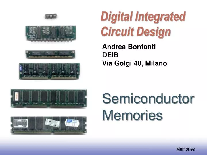
Digital Integrated Circuit Design. Andrea Bonfanti DEIB Via Golgi 40, Milano. Semiconductor Memories. Chapter Overview. Memory Classification. Memory Architectures. The Memory Core. Periphery. Reliability. Semiconductor Memory Classification. Non-Volatile Read-Write Memory.

E N D
Digital Integrated Circuit Design Andrea Bonfanti DEIB Via Golgi 40, Milano Semiconductor Memories
Chapter Overview • Memory Classification • Memory Architectures • The Memory Core • Periphery • Reliability
Semiconductor Memory Classification Non-Volatile Read-WriteMemory Read-Write Memory Read-Only Memory Random Non-Random EPROM Mask-Programmed PROM Access Access 2 E PROM FLASH FIFO SRAM LIFO DRAM Shift Register CAM
Decoder reduces the number of select signals K = log N 2 Memory Architecture: Decoders M bits M bits S S 0 0 Word 0 Word 0 S 1 Word 1 Word 1 A 0 S Storage Storage 2 Word 2 Word 2 A cell cell 1 N words Decoder A K-1 S N-2 Word N-2 Word N-2 S N-1 Word N-1 Word N-1 Input-Output Input-Output ( M bits) ( M bits) Intuitive architecture for N x M memory Too many select signals: N words == N select signals
Array-Structured Memory Architecture Problem: ASPECT RATIO or HEIGHT >> WIDTH + - Amplify swing to rail-to-rail amplitude Selects appropriate - word
Hierarchical Memory Architecture Advantages: 1. Shorter wires within blocks 2. Block address activates only 1 block => power savings
Read-Only Memory Cells BL BL VDD WL WL BL BL WL WL GND MOS ROM 1 MOS ROM 2
MOS OR ROM BL [0] BL [1] BL [2] BL [3] WL [0] V DD WL [1] WL [2] V DD WL [3] V bias Pull-down loads
MOS NOR ROM V DD Pull-up devices WL [0] GND WL [1] WL [2] GND WL [3] BL [0] BL [1] BL [2] BL [3]
MOS NOR ROM Layout Cell (9.5l x 7l) WL0 Programming using the Active Layer Only GND WL1 WL2 Polysilicon GND Metal1 Diffusion WL3 Metal1 on Diffusion BL3 BL2 BL1 BL0
MOS NOR ROM Layout Cell (11l x 7l) WL0 Programming using the Contact Layer Only GND WL1 WL2 Polysilicon Metal1 GND Diffusion WL3 Metal1 on Diffusion BL3 BL2 BL1 BL0
MOS NAND ROM V DD Pull-up devices BL [0] BL [1] BL [2] BL [3] WL [0] WL [1] WL [2] WL [3] All word lines high by default with exception of selected WL
No contact to VDD or GND necessary; drastically reduced cell size Loss in performance compared to NOR ROM MOS NAND ROM Layout Cell (8l x 7l) Programming using the Metal-1 Layer Only WL0 WL1 WL2 Polysilicon WL3 Diffusion Metal1 on Diffusion BL3 BL1 BL2 BL0
NAND ROM Layout Cell (5l x 6l) Programming using Implants Only WL0 WL1 WL2 WL3 Polysilicon Threshold-alteringimplant BL3 BL1 BL2 BL0 Metal1 on Diffusion
V DD BL r word WL C bit c word Equivalent Transient Model for MOS NOR ROM Model for NOR ROM • Word line parasitics • Wire capacitance and gate capacitance • Wire resistance (polysilicon) • Bit line parasitics • Resistance not dominant (metal) • Drain and Gate-Drain capacitance
Equivalent Transient Model for MOS NAND ROM V DD Model for NAND ROM BL C L r bit c bit r word WL c word • Word line parasitics • Similar to NOR ROM • Bit line parasitics • Resistance of cascaded transistors dominates • Drain/Source and complete gate capacitance
Precharged MOS NOR ROM V f DD pre Precharge devices WL [0] GND WL [1] WL [2] GND WL [3] BL [0] BL [1] BL [2] BL [3] PMOS precharge device can be made as large as necessary, but clock driver becomes harder to design.
D G S Non-Volatile MemoriesThe Floating-gate transistor (FAMOS) Floating gate Control Gate Source Drain t ox t ox + +_ n n p Substrate Schematic symbol Device cross-section
20 V 0 V 5 V 20 V 0 V 5 V 10 V 5 V S D S D S D Avalanche injection Removing programming voltage leaves charge trapped Programming results in higher V . T Floating-Gate Transistor Programming
FLOTOX EEPROM Gate Floating gate I Drain Source V 20 – 30 nm -10 V GD 10 V 1 1 n n Substrate p 10 nm Fowler-Nordheim I-V characteristic FLOTOX transistor
V DD EEPROM Cell BL WL Absolute threshold control is hard Unprogrammed transistor might be depletion 2 transistor cell
Flash EEPROM Control gate Floating gate erasure Thin tunneling oxide 1 1 n source n drain programming p- substrate Many other options …
Cross-sections of NVM cells Flash EPROM Courtesy Intel
NAND Flash Memory Word line(poly) Unit Cell Source line (Diff. Layer) Courtesy Toshiba
Select transistor Word lines Active area STI Bit line contact Source line contact NAND Flash Memory Courtesy Toshiba
Read-Write Memories (RAM) • STATIC (SRAM) Data stored as long as supply is applied Large (6 transistors/cell) Fast Differential • DYNAMIC (DRAM) Periodic refresh required Small (1-3 transistors/cell) Slower Single Ended
Q 6-transistor CMOS SRAM Cell WL V DD M M 2 4 Q M M 6 5 M M 1 3 BL BL
CMOS SRAM Analysis (Read) WL V DD M BL 4 BL Q 0 = M Q 1 = 6 M 5 V V V M DD DD DD 1 C C bit bit
CMOS SRAM Analysis (Read) 1.2 1 0.8 0.6 Voltage Rise (V) 0.4 0.2 0 0 0.5 1 1.2 1.5 2 2.5 3 Cell Ratio (CR)
WL V DD M 4 M Q 0 = 6 M 5 Q 1 = M 1 V DD BL 1 BL 0 = = CMOS SRAM Analysis (Write)
VDD M2 M4 Q Q M1 M3 GND M5 M6 WL BL BL 6T-SRAM — Layout
Static power dissipation -- Want R large L Bit lines precharged to V to address t problem DD p Resistance-load SRAM Cell WL V DD R R L L Q Q M M 3 4 BL BL M M 1 2
BL 1 BL 2 WWL WWL RWL RWL M 3 V V X M X 2 DD T 1 M 2 V DD BL 1 C S V D BL 2 V V 2 DD T No constraints on device ratios Reads are non-destructive Value stored at node X when writing a “1” = V -V WWL Tn 3-Transistor DRAM Cell
BL2 BL1 GND RWL M3 M2 WWL M1 3T-DRAM — Layout
C S ------------ V V D = – V = V – V BL PRE BIT PRE C + C S BL 1-Transistor DRAM Cell - Write: C is charged or discharged by asserting WL and BL. S Read: Charge redistribution takes places between bit line and storage capacitance Voltage swing is small; typically around 250 mV.
DRAM Cell Observations • 1T DRAM requires a sense amplifier for each bit line, due to charge redistribution read-out. • DRAM memory cells are single ended in contrast to SRAM cells. • The read-out of the 1T DRAM cell is destructive; read and refresh operations are necessary for correct operation. • Unlike 3T cell, 1T cell requires presence of an extra capacitance that must be explicitly included in the design. • When writing a “1” into a DRAM cell, a threshold voltage is lost. This charge loss can be circumvented by bootstrapping the word lines to a higher value thanVDD.
V V (1) BL V PRE D V (1) V (0) t Sense amp activated Word line activated Sense Amp Operation
Metal word line SiO 2 Poly Field Oxide Diffused + + n n bit line Inversion layer Poly Polysilicon induced by Polysilicon plate plate bias gate 1-T DRAM Cell Capacitor M word 1 line Cross-section Layout Uses Polysilicon-Diffusion Capacitance Expensive in Area
Advanced 1T DRAM Cells Word line Capacitor dielectric layer Cell plate Insulating Layer Cell Plate Si Transfer gate Isolation Refilling Poly Capacitor Insulator Storage electrode Storage Node Poly Si Substrate 2nd Field Oxide Stacked-capacitor Cell Trench Cell