Download
1 / 31
310 likes | 393 Views
Silicon-based tracker system for EIC detector . M.A. Antonioli , P. Bonneau , L. Elouadrhiri *, B. Eng, Y. Gotra , M. Leffel , S. Mandal , M. McMullen, B. Raydo , W. Teachey , and A . Yegneswaran * Thomas Jefferson National Accelerator Facility, Newport News, VA 23606

E N D
Silicon-based tracker system for EIC detector M.A. Antonioli, P. Bonneau, L. Elouadrhiri*, B. Eng, Y. Gotra, M. Leffel, S. Mandal, M. McMullen, B. Raydo, W. Teachey, and A. Yegneswaran* Thomas Jefferson National Accelerator Facility, Newport News, VA 23606 E. Kurbatov, M. Merkin, S. Rogozhin, and S. Voronin Moscow State University, Moscow, Russia M. Holtrop and S. Phillips University of New Hampshire, Durham, NH 03824 FNAL SIDET Facility Saclay/CEA J. Ball F. Sabatie, and S. Procureur
Topics • Introduction • CLAS12 SVT • Proposal • Plan: cost, schedule and collaboration • Summary
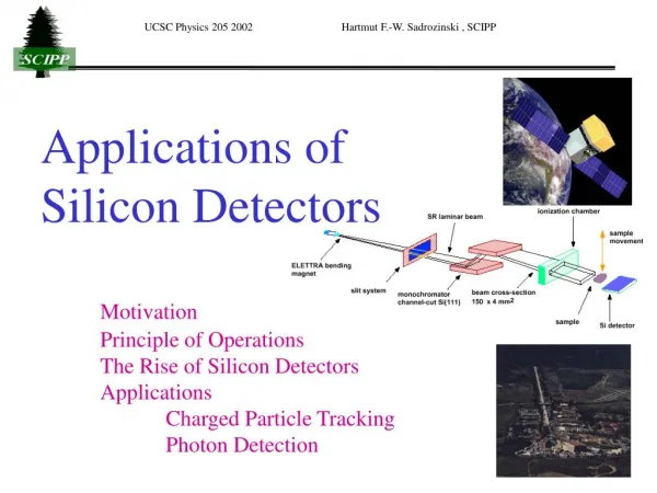
Introduction • Silicon detectors • Ideally suited for tracking close to the interaction region • Capable of handling high rates • Withstand high radiation dose • Provide exceptionally good vertex and tracking resolutions • Standard technology • Highly reliable. • Cost effective • Silicon detectors are used in high-energy physics laboratories across the world • Our Science interest is in the study of Generalized Parton Distributions (GPDs) that require measurement of exclusive processes
CLAS12 in Hall B • Low Threshold • Cerenkov • Forward TOF • Pre-Shower • Calorimeter • Electromagnetic • Calorimeter High Threshold Cerenkov Counter (HTCC) • SC Torus Magnet • Drift Chambers • Moeller Shield • 5 T SC Solenoid • Central TOF • Silicon Vertex Tracker (SVT) • Micromegas • Beam-line: • Raster magnets • Beam Position • Targets • Moeller System, • etc.
CLAS12 – Central Detector CTOF Scintillators • CLAS 12 will have several Cryogenic targets, 2” max radius at CLAS CL (50.8mm) • Minimum ID of the SVT =57mm • CLEARANCE = 6mm • SVT max radius is 179mm • CTOF min radius is 251 mm • CLEARANCE : ~16 mm between Micromegas and SVT tracker • Design for Micromegas • Inside radius 138mm • Note R3 with skin radius max is 133mm • Outside radius 242mm Space for tracking upgrade Micromegas Cryogenic Target
Overview: Detector Design Considerations • Space • Location constrained • by the high threshold Cerenkov counter in the forward direction • by size of polarized target and by the time-of-flight detector in the radial direction • Multiple scattering • Radiation dose • Heat load • Placement tolerances
Design of SVT • Four region barrel • Region 1: 10 modules • Region 2: 14 modules • Region 3: 18 modules • Region 4: 24 modules (separately supported to allow dismount and replacement with Micro Megas Detector) • Simulations indicate that this configuration, three silicon double layers and three Micromegas double layers, dramatically improves the vertex, angular, and tracking resolutions. • All modules for all Regions are identical • Operating Temperature 21oC • Low mass inside acceptance region X0 ~1%
Geometry Implementation in GEMC Silicon 320 Epoxy 100 Bus Cable 31 Carbon Fiber 200 Rohacell 1250 We have a full, realistic implementation of the SVT and Micromegars in the Geant4 simulation that includes electronic noise, charge sharing and physics background For CLAS12 configuration. The simulation and reconstruction framework in place, could be extended to simulate the EIC configuration to calculate rate and radiation doses.
Overview: Rates and Radiation Dose • GEMC Detector Simulation • Includes electro-magnetic and hadronic backgrounds and noise • Rates estimated for LH2, LD2, C, Fe, and Pb targets • For L = 1035 cm-2s-1 • Rates from carbon target • Threshold E ≈ 40 KeV • Hadronic rate : ~5 MHz • Total rate: ~16 MHz • Strip hit rate (R1, 6.3 KHz), (R2, 4.5 KHz), (R3, 3.5 KHz), (R4, 2.6 KHz) • Radiation dose for carbon target • 50 % operation • 15 years duration • ~2.5 Mrads
Design Overview: SVT Module • Pitch Adapter • 156 µm to 50 µm • Metal on glass technology Sensor • All modules have 3 types of sensors • Hybrid, Intermediate, and Far • Sensors cut from 6 inch wafers • 2 sensors/wafer • All sensors have the same size • 111.625 mm × 42 mm FSSR2 ASIC • Developed for BTeV • Readout cable • Hybrid Flex Circuit Board • Based on CDF and D0 designs • Backing structure • Composite structure • Rohacell and Carbon Fiber • Based on CDF and D0 designs
Sensor Design • Sensors design based on proven and reliable designsused at other labs • Comparison study of sensor designs performed for: • CDF, D0, ATLAS, CMS, GLAST • 50+ electrical and mechanical design parameters were reviewed. • Contract with Hamamatsu in place, sensor delivery in • progress will be completed by October 31, 2012.
Sensor Specifications –Mechanical Outer size 42.000 mm x 111.625 mm Active area 40.032 mm x 109.955 mm Dicing tolerance ± 20 µm # of readout strips 256 # of intermediate strips 256 Implant strip pitch 78 µm Readout strip pitch 156 µm Implant strip width 20 µm Aluminum strip width 26 µm Implant width / pitch ratio 0.256 Angle of strips 0°(strip 1) to 3°(strip 256) Overhang of Al strip 3 µm (on each side)
Design Overview: FSSR2 • Fermilab Silicon Strip Readout Chip – Rev.2 • 128 channels / chip, 50 μm input pitch • Data-driven architecture - self-triggered, time-stamped • 1 MHz input rate with < 2% missed • Beam Cross Over (BCO) clock: from 128 ns • DAQ synchronized with timestamp clock • Zero-suppressed data readout • 1-6 programmable serial outputs (for hit data output) • Double Data Rate (DDR) output • Maximal data output rate 840 Mbits/s • Anticipated data rate ~ 200 Mbits/s • Data readout clock: use 70 MHz • 24 bit data format for ‘hit’ channel • 12 bit Address • 8 bit BCO clock counter • 3 bit ADC • 1 Sync • Power consumption < 4 mW / channel • Single 2.5 V supply separated on chip • Designed to handle 5 Mrad
Module Components: HFCB • Hybrid Flex Circuit Board (HFCB) Data Power Power FSSR2 Data FSSR2
Proposal • For the EIC silicon tracking system • Build, initially, a 66-cm long module—two standard modules placed end to end—and read out from both ends. • Investigate the mechanical stability of the long module • determine how to maximize the signal-to-noise ratio of the module. • Conduct extensive tests, including a full-scale test with the CLAS SVT and CLAS Micromegas • Understand and optimize the compatibility of these two tracking detectors • Readout all strips including intermediate strip which will require new readout board with 4 ASICs • Perform detail Geant 4 simulation
Collaboration Strategy • Jefferson Lab – JLab • Design module and design of the mechanical support • Development of readout & system integration • DAQ/Software • Procurement of all part • FNAL/MSU/UNH/Jlab • Simulation (background and radiation doses,…) • Production module assembly & test • Production module laser testing • FNAL/JLab • Module Assembly • Wire-bonding • CEA/Saclay • Provide Micromegas Module with readout and testing procedures • Charge particle tracking
Infrastructure • Class 10,000 clean room dedicated for module fabrication, • Associated infrastructure • granite table wire bonder, • test and measurement equipment, • probe station • dark box needed to evaluate the silicon modules and • environmental chamber • dry-storage systems • SVT and Micromegas prototypes
JLab/ FNAL Infrastructure JLab Infrastructure FNAL SIDET Facility
Funding Profile Request • Year 1 Year 2 Year 3 Total • Labor $50K $50K $50K $150K • Hardware $25K $25K $25K $75K • Travel $8K $7K $7K $22K • Total $83K $82K $82K $247K Labor includes mechanical designer and electrical designer Labor for simulation and testing Procurement includes additional sensors (4 of each type) readout board
Three Year Plan • Year 1 • Procure backing structure materials for the silicon module • Build module • Test module performance • Work on optimizing signal-to-noise ratio. • Recruit post-doc • Year 2 • Procure components to install the silicon module in close proximity to a curved Micromegas prototype • Start compatibility tests. • Year 3 • Complete compatibility tests on the module and the Micromegas prototype • Proceed to full-scale compatibility studies with CLAS SVT and CLAS Micromegas.
Summary • Silicon based tracking system • Appropriate and cost effective • Sensor mask already made, contract with Hamamatsu in place • Contract with FNAL in place for module production • Chips tested and in hand • Backing structure component and cooling system available • Essential R&D • Study long modules ~66 cm • Investigate interaction between Micromegas and SVT • Micromegas will be provided by Saclay (Approved EIC R&D proposal) • Strong Collaboration • JLAB / MSU / CEASaclay- IRFU / UNH / Fermilab • Extensive experience
Sensor Specifications:Electrical Full depletion voltage 40<V<100 (25° C@<45% RH) Interstrip capacitance <1.2 pF/cm Leakage current (@ depletion V) <10 nA/cm2 Strip to back side capacitance < 0.2 pF/cm Interstrip isolation (@150 V) >1 GΩ Resistance of Al strips < 20 Ω/cm Coupling capacitance > 20 pF/cm Total (strip) capacitance ≤ 1.3 pF/cm; (Ctot = 2*Cint + Cback @ 1 MHz) Value of poly-silicon bias resistor 1.5 MΩ Single strip DC current < 2 nA CLAS-Note 2009-020, Silicon Micro-Strip Sensors for the Hall B CLAS12 SVT
Radiation Dose on Silicon ------------ carbon Layer 1a Fluences: ------------ particles GeV/smrad/srad/year pi- 229 0.112763 3556 e- 209 0.102942 3246 gamma 5236 2.57438 81185 n 47 0.0232453 733 e+ 58 0.0286764 904 pi+ 365 0.1798 5670 p 9967 4.89975 154518 all 19468 9.57049 301814 301 Krad / year (2 years on the floor) 2.2 Mrad for 15 years on Carbon Within acceptable limits of 5 Mrad LodovicoRatti, Massimo Manghisoni, Valerio Re, GianlucaTraversi, Andrea Candelori RADECS 2005 Nuclear Instruments and Methods in Physics Research A 466 (2001) 354–358
Radiation Dose on Chip ----------------------- iron Layer chip_r1 Fluences: ----------------------- particles GeV/smrad/srad/year pi- 0 0.0146573 462 e- 8 0.257076 8107 gamma 2 0.0822083 2592 n 0 0.00509819 160 e+ 0 0.0307166 968 pi+ 0 0.0261282 823 p 3 0.0949537 2994 all 20 0.635616 20044 20 Krad / year (2 years on the floor) 0.15 Mrad for 15 years on Iron Within acceptable limits of 5 Mrad LodovicoRatti, Massimo Manghisoni, Valerio Re, GianlucaTraversi, Andrea Candelori RADECS 2005 Nuclear Instruments and Methods in Physics Research A 466 (2001) 354–358
Sensor Design: Layout of Sensors U Layer V Layer Graded pitch design; Stereo angle from 0°- 3° CLAS-Note 2009-022, Sensor Mask Layout Procedure
Cold Plate Provides mechanical support to the SVT Provides cooling for the electronics on the modules Material : Noryl - 30% Glass Filled Coolant: Water Coolant temperature: 15oC Flow rate: 3 LPM (Twater ~0.6oC) Heat Sink Material : Copper Sub-atmospheric system is also being considered Coolant Channel Copper Insert