Download
1 / 69
780 likes | 1.11k Views
Silicon Detector Applications are described her.

E N D
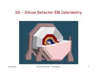
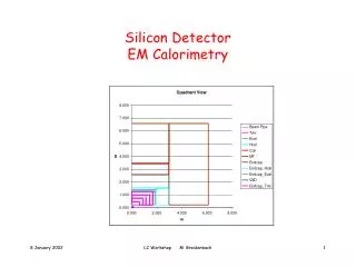
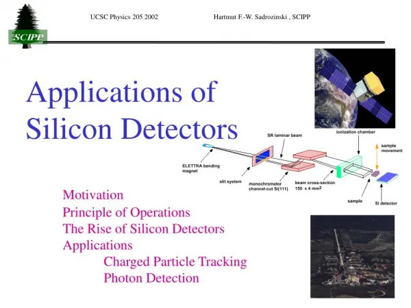
Applications of Silicon Detectors Motivation Principle of Operations The Rise of Silicon Detectors Applications Charged Particle Tracking Photon Detection
Primary Z Vertex Detached Vertexes In B andanti-B Precision Particle Tracking Detectors • In Particle Physics, many new phenomena tend to be associated with heavy quarks. • The Higgs search will depend on tagging heavy flavor jets, • CP violation is being measured in the b system. • Heavy quarks have a finite life time t, and can be identified by the decay length in the lab Dz gbct (= 250um in BaBar). • This requires detectors in close proximity (few cm) of the beams • with an intrinsic position resolution of 10 - 25um. • High particle densities in “jets” require fast, fine-grained detectors. • This is possible only with semiconductor detectors. • Vertexing precision depends on: • distance of the detectors from the interaction point, • the lever arm, and the • intrinsic position resolution • of the detector
Particle Tracking Detectors for Theorists Choose a fine-grained detector to localize charged particles: Passing of particle leaves a trail of temporal ionization (>10,000e) (see next) Take advice from your local guru and collect it electronically -> apply electric field, record tiny current Is (<uA in 10 ns) = signal Problem: Resistivity of detector material : In = V/R gives large current Way out: block current with capacitor Problem: large current still gives background noise ~ In Ways out: Ultra-high resistivity materials (Diamonds, SiC, few Mohm-cm) Reverse biased diode on Si (few kOhm-cm, industry grade)
W Electrostatics of Silicon Strip Detectors Resistivity given by concentration of dopants N (donors or acceptors) . Charge can’t be collected from the conductive bulk : have to deplete it of mobile carriers (e), leaving the bulk charged Depletion depth depends on bias voltage Capacitance measured the depletion depth 1/C2 VBias
ik = -qmE(x)•Fk(x) Dynamics of Silicon Strip Detectors Charge Collection: Drifting Charges Induce Charges on Electrodes Drift Velocity E operating field, m mobility Induced Charges Vql : Weighting Potential (Ramos, 1937) Signal Current due to drifting charges Fk(x) : Weighting Field (Cap) Collection Time Scale Signal ends when charge arrives at the strip
Further Reading for the Curious http://britneyspears.ac/lasers.htm
~1/b1.5 Rad measure p MIP Signal in Tracking Detectors Charged Particle Energy Loss (aka Stopping Power, Linear Energy Loss LET) Bethe-Bloch Signal-to-Noise Ratio: Signal ~ Thickness Noise ~ Area, 1/ts Directional Information compromised by Multiple Scattering Multiple Scattering angle -> Thin, low z materials -> Improves at High Energy Radiation Length Xo
Readout electronics (S/N typically > 20) 25-200 mm Al SiO2 p+ implant at ground Depletion region. Charged particle traversing region produces ~80 electron/hole pairs per micron. 300-400 mm holes n+ implant Al at ~ 100V Properties of Silicon Strip Detectors Reverse Bias of junction: only thermal current generation Scale : Band gap 1.12eV vs. kT = 1/40eV: huge Boltzmann factor Cooling needed only in ultra-low noise applications. Wafer thickness 300um = 0.3%RL: 23k e-h pairs Depletion Voltage ~ thickness2 : <100V Collection Time of e-h pairs: ~20ns Area is given by wafer size: 4” & 6” => Ladders
n n n p p n n n Evolution of Silicon Detectors Double-sided Large Area Si Drift 3-D Hybrid Pixels Monolythic: CCD, MAP
The Rise of Silicon Detectors Development of Area of SSD and # of Electronics Channels follow Moore’s Law Larger - CMS 10M Channels, 230m2 Faster - ATLAS 22ns Cheaper - CMS ~$5/cm2 o o O: SCIPP o o o o
Edge joint and wire bonds before encapsulation Area [m2] The Rise of Silicon Detectors Limited Resources (Power) in Space Long Ladders possible with: Bonding and Encapsulation
The Rise of Silicon Detectors Trends in the Cost of Silicon Detectors Cost of processing wafers reduced ~ 4x Increased Area 4” -> 6” Better utilisation of area Improved Quality e.g. GLAST detectors: <2nA/ cm2 <2*10-4 bad channels (Guestimates by HFWS)
DC (Drift Chamber) vs. SSD (Silicon Strip Detector) What to do next?
Typical Low Tech University Jobs What to do next?
Typical Low Tech University Jobs What to do next?
Tracking Milestones: Fixed Target That’s how it all began Fixed Target experiments with high rates: Na11 (ACCMOR), Na14, E706. E691 Detect heavy decaying particles through their finite decay distance Silicon Detectors ~ 5cm x5cm What to do next? Fanout-Cables Amplifiers
ALEPH {A. Litke et al) Tracking Milestones: Vertex Detectors The big step forward in Mark2: ASIC’s(A. Litke et al) Vertex Detector Paradigm ASIC’s, Few thin layers, Close in. Every LEP Experiment has a Vertex Detectors: Double-Sided AC-coupled
Primary Z Vertex SLD Detached Vertexes In B andanti-B Tracking Detectors: CCD 300M pixel CCD device for SLD (A. Seidem, T. Schalk, B. Schumm) Few um resolution in two coordinates Follow the (Industrial) Leader.. X
Tracking Milestones: Speed and Rad.Hardness LPS at HERA (D. Dorfan, N. Spencer, J. DeWitt, N. Cartiglia, E. Barberis, A. Seiden, D. Williams, HFWS ) “Fixed Target” at Collider Importance of Electronics: rad hard fast low noise low power 56 planes, 50k channels Elliptical shapes! 2mm from 800GeV beam 2 chip set: Bipolar+CMOS Hadron-Machines: Radiation Damage
Temperature Range : -17oC (cooling pipe) to +16oC (ASICs) Tracking Milestones: Highest Luminosity LHC ATLAS: Silicon Tracker (A. Seiden, D. Dorfan, A. Grillo, N. Spencer, S.Kachiguin, F. Rosenbaumm, M. Wilder, HFWS) Simple Detectors,Optimized Electronics Thermal management Vertex Detector Inner Detector Change in Paradigm: coverage of large area electronics inside tracker volume
Tracking Milestones: Highest Luminosity LHC • Silicon has arrived: • all Silicon Inner Detector • Si Area 223m2, • 6” Wafers – • (Ariane Frey et al) Continued Paradigm Change: >20 layers of Si, outside radius : ~1.1m ~1R.L. in tracking volume almost exact size of old wire chambers!
Technology Transfer of Silicon Detectors Protons Biology Small-scale Large-scale X-rays Medicine g-Rays Space Science C.Rays Charged Particle Tracking in HEP Industrial Base
Si Tracking in Space: Sileye Cosmonaut Adveev on Mir Sileye Investigate light flashes seen by Cosmo-/Astro-nauts during Orbital flights. Occurrence of flashes well correlated with areas of high flux of Cosmic ray particles.
conversion foil particle tracking detectors e– e+ Photon Detection in Astronomy: Direction, Direction,.. Photon Attenuation Coefficient Attenuation of Phtotons N(x) = Noe- l x l varies by 105! • Attenuation coefficient • = (7/9)/Xo < 0.3% Conversions in one SSD! Optical- X-rays Need Focus: Lenses Mirrors Collimators Coded Masks Proximity Pair- Production Direction anticoincidence shield Compton Partial Direction • calorimeter • (energy measurement)
charged particle anticoincidence shield conversion foils particle tracking detectors e- e+ • calorimeter • (energy measurement) GLAST: Pair Conversion Telescope Gamma-rays convert into e+e- pairs, are tracked and their energy measured Gamma is reconstructed from e+e- tracks Reconstruct Vertex New Paradigm:Add material into tracking volume: Maximize Number of Converters Converter Thickness t Conversion Probability ~ t Pointing RMS ~ t
An Astro-Particle Physics Partnership Exploring the High-Energy Universe GLAST Gamma-Ray Large Area Space Telescope Design Optimized for Key Science Objectives • Understand particle acceleration in AGN, Pulsars, & SNRs • Resolve the g-ray sky: unidentified sources & diffuse emission • Determine the high-energy behavior of GRBs & Transients Proven technologies and 7 years of design, development and demonstration efforts • Precision Si-strip Tracker (TKR) • Hodoscopic CsI Calorimeter (CAL) • Segmented Anticoincidence Detector (ACD) • Advantages of modular design • NASA, DoE, DoD, INFN/ASI, Japan, CEA, IN2P3, Sweden Challenges of Science in Space • Launch • Limited Resources • Space Environment Resolving the g-ray sky
Tracker Grid Thermal Blanket ACD DAQ Electronics Calorimeter GLAST Large Area Telescope (LAT) • Array of 16 identical “Tower” Modules, each with a tracker (Si strips SSD) • 10,000 SSD • 83m2 area • ~1M channels, • ~ 5M wire bonds • A calorimeter (CsI with PIN diode readout) and DAQ module. • Surrounded by finely segmented ACD (plastic scintillator with PMT readout).
648 GLAST Silicon Tracker SCIPP (R. Johnson, W. Atwood, W. Rowe, A. Webster, N. Spencer, S. Kachiguine, W. Kroeger, M. Hirayama, M. Sugizaki, B. Baughman, HFWS) Tower Structure (walls, fasteners) Engineering: SLAC, Hytec Procurement: SLAC I SSD Ladder Assembly Italy I SSD Procurement, Testing Japan, Italy, SLAC I 10,368 Tower Assembly and Test SLAC (2) Italy (16) 2592 Tray Assembly and Test Italy I 342 Electronics Design, Fabrication & Test UCSC, SLAC I 18 342 Composite Panel & Converters Engineering: SLAC, Hytec, and Italy Procurement: Italy I Cable Plant UCSC I Most Production and Assembly Steps done in Industry = I Testing: Academic & Research Institutions
2 delicate hands 4 trays, 10 eyes & 10 hands 17 trays! Typical High Tech University Jobs 2 trays and 2 observers All done and all smiles.
Astrophysics: Imaging, Tracking Medicine: Imaging X-talography: Imaging Nuclear Physics X-Spectroscopy Particle Physics: Tracking Gravitation Electro-magnetic Weak Strong Application of Silicon Detectors: No Limits We build instruments to explore the structure of our world from Quarks (<10-20m) to the entire Universe (>1028m). Silicon Detectors are used for experimentation at every scale. The largest SSD systems are in Astro- and Particle Physics. We trying to play catch-up in Life Sciences.
~ 1,000,000 TKR Channels~ 6,000,000 encapsulated Wire Bonds TKR Interconnects: Industry Job
GLAST Front-End Electronics ASIC • Binary Readout: • Low-power (~200uW/channel) • Peaking time ˜ 1.3 ms • Low noise (Noise occupancy <10-5) • Threshold set in every ASIC • Separate Masks for Trigger and Readout in every Channel • Trigger = OR of one Si plane (1536 channels) Electron Events Pulse Height: Time –over-Threshold on the OR of every Si plane Distinguish single tracks from two tracks in one strip Photon Events
Prototyping of the GLAST SSD The SSD design has been finalized and procurement is underway 11,500 SSD inlude 10% Spares Qualify Prototypes from HPK (experience with ~5% of GLAST needs) 0.1*specs +340 Additional Prototypes: Micron (UK), STM (Italy), CSEM (Switzerland)
Some Basic Questions in Radiobiology: • It’s the DNA, stupid! • Are there different classes of damage depending on the Linear Energy Transfer (LET) and number of ionizations/DNA molecule? • By-stander effect: Damage is being transmitted to distant cells • Effect of OH- radicals in the damage process • Improve dosimetry of proton beam for cancer therapy Collaboration (NASA-CalSpace) Loma Linda U. & UCSC (SCIPP & CfO) (A. Seiden, R. Johnson, W. Kroeger, P. Spradlin, B. Keeney, HFWS)
Ionization event (formation of water radicals) Light damage- reparable Primary particle track delta rays e- OH• Water radicals attack the DNA Clustered damage- irreparable The mean diffusion distance of OH radicals before they react is only 2-3 nm Radiation Damage DNA
Project Goals • Establishment of a nanodosimetric gas model to simulate ionizations in DNA and associated water • Plasmid-based DNA model to measure DNA damage • Develop models to correlate nanodosimetry with DNA damage
Principle of Nanodosimetry (Statistical Approach) 1nm solid 1 mm @ .001 atm (~1 torr) 1 um @ 1 atm X 1000 X 1000 DNA Propane gas Low pressure propane gas
Setup and Silicon Modules VME CRATE Localization of Protons 2 Silicon Strip Detector (SSD) Modules ND Vessel SSD DAQ PC W/ DAQ PCI Card Ion counter
0 -5 millivolts -20 0 1 2 3 microseconds ND Ion Cluster Spectra Event with 6 ions A primary particle event is followed by an ion trail registered by the ion counter (electron multiplier) For low-LET irradiation, most events are empty
ND Ion Cluster Spectra Ion Cluster Spectra Ion cluster spectra depend on particle type and energy as well as position of the primary particle track The average cluster size increases with increasing LET
Radiobiological Model • Plasmid (pHAZE) • Irradiation of thin film of plasmid DNA in aqueous solution • Three structural forms: • superhelical (no damage) • open circle (single strand break) • linear (double strand break) • Separation by agarose gel electrophoresis • Fluorescent staining and dedicated imaging system
What is needed? Global (Nanodosimetry): Well in Hand ? Correlation needed! Tag individual Interaction, Investigate Damage in detail on struck molecules Local: Needs Improvement No Radiometry Measurement Correlated with Damage on individual DNA Molecule
Particle Tracking Silicon Microscope (PTSM) Protons produce damage AND identify damaged organism Transfer to Automated Microscope when Occupancy ~ 10% Worms in Liquid Phase (directly on SSD) Double-sided SSD: x-y coordinate, Energy, “Cluster characteristics”. Assay with Automated Microscope using stored x-y coordinates
Chromosome structures in the gonad of the adult hermaphrodite
0-8h: II (early embryogenesis) + III (diakinesis oocyte) 8-24h: III + IV + V + VI (diplotene to pachytene nuclei)