Download
1 / 15
150 likes | 153 Views
This article explores the use of bonding techniques in micromachining for the assembly of individually micromachined parts to form complete structures. It discusses different bonding processes, such as fusion bonding and anodic bonding, along with optimized bonding methods and the annealing treatment required. It also covers bonding of silicon-based materials and quality control for silicon-on-insulator wafers. Examples of wafer bonded pressure sensors, thermally isolated infra-red detectors, and wafer bonded accelerometers are provided.

E N D
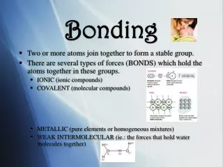
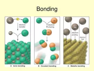
BONDING • The construction of any complicated mechanical device requires not only the machining of individual components but also the assembly of components to form a complete set : in micromachining, bonding techniques are used to assemble individually micromachined parts to form a complete structure. • When used in conjunction with micromachining techniques, wafer bonding allows the fabrication of 3-dimensional structures which are thicker than a single wafer. • Several processes have been developed for bonding silicon wafers. The two most important processes are fusion bonding and anodic bonding.
Fusion Bonding • In its simplest form the wafer fusion bonding process includes mating of a wafer pair, which has surfaces of both wafers hydrated, at room temperature and subsequent annealing. • A major concern of bonding processes is non-contacting areas which are generally called voids. Voids are caused by particles, organic residues, surface defects, and inadequate mating. • Therefore optimized bonding includes : (i) Wafer surface inspection. (ii) Surface cleaning. (iii) Mechanically controlled, aligned mating in a particle- free environment.
Annealing Treatment Three annealing temperature ranges are of interest : • (i) T < 450 °C For post-metallization wafers. • (ii) T < 800 °C. For wafers with diffusion dopant layers (e. g., high boron concentration etch-stop). Results in a sufficient bond strength for subsequent processes such as grinding, polishing, or etching. • (iii) T > 1000 °C. For wafer bonding before processing. Annealing at temperatures above 1000 °C for several hours should result in almost complete reaction of the interface. A 1000 °C anneal for ~ 2 hrs gives sufficiently high bond strength for all subsequent treatments; it is not possible to separate the two bonded wafers without breaking the silicon.
Fusion of Silicon-Based Materials • Bonding of poly-Si, silicon dioxide, or silicon nitride to Si proceeds in a manner similar to silicon-to-silicon bonding. • In the case of poly-Si bonding to Si a polishing step for the two surfaces to be bonded is necessary; this polishing step produces two smooth defect-free surfaces. • Because of dissimilar mechanical characteristics of the different materials, the yield of void free wafers can be significantly reduced by wafer bow or defects caused by stress during thermal treatment. • Bonding of wafers covered with a thin thermal oxide or a thin silicon nitride results in homogeneous bonded wafers, while wafers with thicker oxide or nitride films develop voids during annealing.
Silicon-On-Insulator (SOI) Wafer by Fusion Bonding • (a) A heavily doped layer is diffused or implanted into the first Si wafer. A thin lightly doped layer is then grown atop the heavily doped layer. • (b) A silicon dioxide film is thermally grown on the second wafer. • (c) The surfaces of the two wafers are cleaned, contacted and annealed to form a permanent bond. The first wafer is etched until the heavily doped layer is reached and the etch stops. • (d) The heavily doped layer is then removed leaving a bulk quality film.
Anodic Bonding Silicon-to-silicon anodic bonding is a bonding technique used to seal silicon together by use of a thin sputter-deposited glass layer. A heat chuck element with an electrode capable of supplying high voltage across the structure to be bonded. The system may automatically control the temperature and power supply during the bonding process.
After wafer cleaning and polishing, one of the wafers is initially given a few microns thick glass film (sputtered). • The glass coated wafer is placed atop the support wafer which rests on the aluminum chuck of the bonding equipment. • The wafers are sealed together with anodic bonding at temperatures below 400 °C with an electrostatic DC voltage of 50 to 200 V. The negative electrode is connected to the top sputter-coated wafer. • Typically the bonding process is terminated within 10 to 20 minutes and is usually performed in air at atmospheric pressure.
Example (8) : Wafer Bonded Pressure Sensor • (a) Micromachine a V-groove in the first wafer. • (b) Bond to a second wafer. • (c) Thin the second wafer (etching or lapping) and fabricate sensor electronics. • (d) Thin the first wafer to complete pressure sensor chip. Petersen etal., Proc. IEEE Solid State Sensors and Actuators Workshop (1988), 978-981
Example (9) : Thermally Isolated Infra-Red Detector over Sealed Cavity • A cavity is etched in the first Si wafer. • A silicon nitride film (for thermal isolation) is deposited on the surface of a second Si wafer. • The two wafers are bonded with the nitride in between the two Si bulk materials. • The nitride coated wafer is etched back to leave a thin single-crystal Si layer where the radiation sensor is formed. Bang etal. in Appl. Phys. Lett. (1995).
Example (10) : Wafer Bonded Accelerometer • The accelerometer is micromachined in one Si wafer. • This wafer is then bonded to a second Si wafer where the tab stops were micromachined. • The two Si wafers were then bonded to a glass substrate. Barth etal., Proc. IEEE Solid-State Sensors and Actuator Workshop, (1988) pp. 35-38.
Example (11) : Electrostatically-Actuated Micro-valve The device is a pressure balanced micro-valve where several fusion bonded Si layers were combined to form a valve suitable for controlling high-pressure fluid flow. Huff etal., 7th Int. Conf. Solid-State Sensors and Actuators, (1993) pp.98-101.
Possible Configurations Fabricated With DSE and Bonding Techniques
Possible Configurations Fabricated With DSE And Bonding Techniques