Download

1 / 20
200 likes | 388 Views
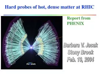
Design & production of silicon sensors for phenix mpc -ex. Jiman Ha (Yonsei Univ.) For PHENIX MPC-EX collaboration. MPC-EX. 참여그룹 국외 : Brookhaven Nation Laboratory, Iowa State University, University of California-Riverside, Los Alamos National Laboratory

E N D
Design & production of silicon sensors for phenixmpc-ex Jiman Ha (Yonsei Univ.) For PHENIX MPC-EX collaboration
MPC-EX • 참여그룹 • 국외 : Brookhaven Nation Laboratory, Iowa State University, University of California-Riverside, Los Alamos National Laboratory • 국내: Yonsei University, ETRI, EwhaWomens University, Hanyang University, Chonbuk National University • 발표관련 기여 • Sensor design : BNL, Yonsei & ETRI • Sensor production : Yonsei & ETRI • Sensor test : Yonsei, EwhaWomens University
MPC-EX for PHENIX • Application as a pre-shower for EMCal (Electromagnetic calorimeter)
Electromagnetic Shower (A schematic view) PAD STRIP W SEG0 SEG1 SEG2 ~1X0 x 20 -RM<y<RM y (EM Shower by single e) z
Sensor Geometry 6.2 cm Total # of PADs = 128 # of PAD column =32 0.18cm 6.2 cm 1.5cm # of PAD row =4
SOME DESIGN DETAILS Edge Rounding PADs of Sensor Bonding PADs Biased/Floating Guardring Floating Guardring (3 layer structure)
How do we make it? (CMOS process) Metal layer deposition High purity Si wafer Oxidation Passivation Oxide layer deposition Etch for contact Ion implant
Capacitance–voltage Relation • Wafer– Resistivity = 6, 9, 12, 18kΩ∙cm / Thickness = 405μm, Orientation = <100> • Full Depletion Voltage = 90V(6kΩ∙cm),60V(9kΩ∙cm),45V(12kΩ∙cm),30V(18kΩ∙cm ) Full Depletion Bias Voltage (V)
Current-Voltage relation(ongoing work) • No breakdown upto200V but somewhat large leakage current Leakage current abruptly rise! Leakage current flows from no bias guardring No Breakdown ! Full Depletion
Current-Voltage relation (ongoing work) • No breakdown upto200V and reduced leakage current . No Breakdown! Full Depletion
Summary • MPC-EX is a pre-shower detector in Si/W sandwich structure. • We designed and fabricated a prototype of the relevant Si sensor.