Download
1 / 42
500 likes | 1.08k Views
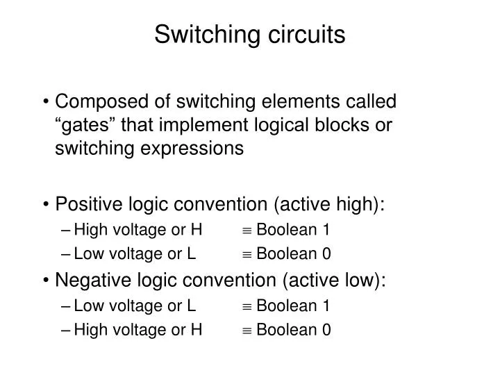
Switching circuits. Composed of switching elements called “gates” that implement logical blocks or switching expressions Positive logic convention (active high): High voltage or H Boolean 1 Low voltage or L Boolean 0 Negative logic convention (active low):

E N D
Switching circuits • Composed of switching elements called “gates” that implement logical blocks or switching expressions • Positive logic convention (active high): • High voltage or H Boolean 1 • Low voltage or L Boolean 0 • Negative logic convention (active low): • Low voltage or L Boolean 1 • High voltage or H Boolean 0
Switching circuits • Logic variables inputs/outputs “signals” • Signals “asserted” when the voltage level assumes the corresponding “1” value • Positive logic asserted by H • Negative logic asserted by L • Logic variables are written complemented when they are active low • Active high signals: a, b, c • Active low signals: ā, ē, ū
Logic gates • Logic gates switching functions • Gate symbols – two sets
Logic gates • Gate symbols – two sets
Logic gates • The NAND logic function and gate
Logic gates • The NAND gate can be used to implement all 3 elementary operations of switching algebra: AND, OR, NOT
Logic gates • The set {AND, OR, NOT} implements any switching function (by definition): it is functionally complete • Therefore, the “NAND” gate can be used to implement any switching function • It is functionally complete, or “primitive”
Logic gates • The NOR logic function and gate
Logic gates • The NOR function can be used to implement all 3 elementary operations of switching algebra: AND, OR, NOT • It is functionally complete too
Logic gates • The NOR logic function and gate
Logic gates and equivalence • CMOS is “inverting” logic • NOR and NAND are easier to implement than OR and AND • They are implemented as NOR or NAND followed by an inverter • More than one representation is possible for the same switching function • Different circuits of logic gates might perform the same switching function • Simpler networks are preferable • Need to analyze for equivalence and transform
Logic gates and equivalence • Equivalent logic networks
Logic gates and equivalence • Proving the equivalence
Digital circuits • Analysis • Given a circuit, abstract the Boolean function it is implementing and try to improve the implementation or verify the function • From gate diagrams • From timing diagrams • Synthesis • Given a switching function, obtain the corresponding switching network
Analysis • Timing diagram
Analysis • Truth table
Analysis • Switching network
... derives truth table Combinational analysis
Signal expressions Multiply out:F = ((X + Y¢) × Z) + (X¢× Y × Z¢) = (X × Z) + (Y¢× Z) + (X¢× Y × Z¢)
Any number of manipulations can yield equivalent circuits e.g. F = ((X + Y’)Z) + X’YZ’ Note: [X’YZ’]Z = 0 (X + Y’)X’YZ’ = 0 (X’YZ’)(X’YZ’) = X’YZ’ So, F = [(X + Y’) + X’YZ’][Z + X’YZ’] =(X + Y’ + X’)(X + Y’ + Y)(X + Y’ + Z’)(Z + X’)(Z + Y)(Z + Z’) =(1)(1)(X + Y’ + Z’)(X’ + Z)(Y + Z)(1) = (X + Y’ + Z’)(X’ + Z)(Y + Z) Circuit:
Conclude: given circuit ==> many equivalent equations circuit does not determine equation
Two-level AND-OR Two-level NAND-NAND Three-level equivalent Also, equation does not determine circuit:
Combinational analysis given circuit, determine function Combinational synthesis given function, determine circuit
Prime number detector: F = (1, 2, 3, 5, 7, 11, 13) AND-OR design
Alarm: Derive truth table or expand: A = P + E EX’ (W D G)’ = P + E EX’ (W’ + D’ + G’) = P + E EX’ W’ + E EX’ D’ + E EX’ G’
NANDs, NORs have fewer transistors than ANDs, ORs AND-OR converts readily to NAND-NAND
Bubble-pushing produces non-standard gate Solution: inverters
Bubble-pushing produces non-standard gate Solution: inverters
Bubble-pushing produces non-standard gate Solution: inverters
Synthesis • SOP functions -> AND – OR networks • POS functions -> OR – AND networks • Not always possible to design directly • Fan-in and out restrictions • Most designs are modular and multi-level • Modern designs are too complex • Design and testing by computers • VLSI - CAD
Logic simulation • Two states only for an ideal logic signal • Two gates driving the same line in opposite directions • Input left not connected or “floating” • Third state ‘X’ is added to the set of states • Truth tables change
Synthesis approaches illustrated to this point: Truth table derivation of minterms Ad hoc construction of logic equation Need systematic approach that minimizes hardware Karnaugh maps Quine-McCluskey algorithm