Download
1 / 32
320 likes | 595 Views
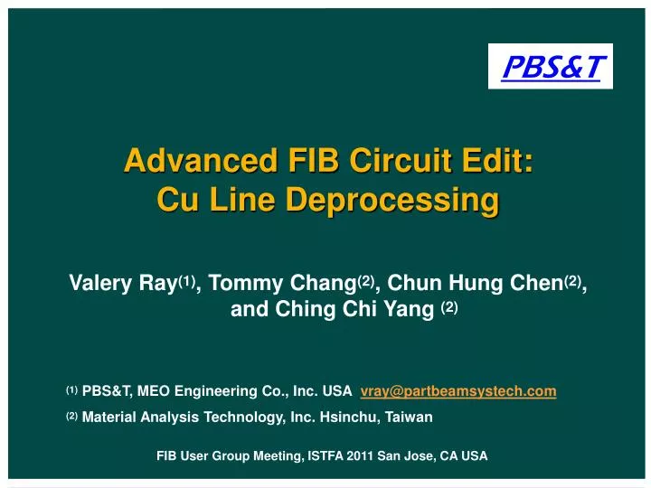
PBS&T. Valery Ray (1) , Tommy Chang (2) , Chun Hung Chen (2) , and Ching Chi Yang (2) (1) PBS&T, MEO Engineering Co., Inc. USA vray@partbeamsystech.com (2) Material Analysis Technology, Inc. Hsinchu, Taiwan. Advanced FIB Circuit Edit: Cu Line Deprocessing. Outline.

E N D
PBS&T Valery Ray(1), Tommy Chang(2), Chun Hung Chen(2), and Ching Chi Yang (2) (1) PBS&T, MEO Engineering Co., Inc. USA vray@partbeamsystech.com (2) Material Analysis Technology, Inc. Hsinchu, Taiwan Advanced FIB Circuit Edit:Cu Line Deprocessing FIB User Group Meeting, ISTFA 2011 San Jose, CA USA
Outline • Cu Deprocessing Methods • 65nm-node Device, Thick Cu Line 50KV Process • 40nm-node Device, Thick Cu Line 30KV and Thin Cu Line 50KV Process • Dummy Cu example 9/17/2014 FIB User Group Meeting, ISTFA 2011 San Jose, CA USA 2
Cu Deprocessing Difficulties • GAE is impossible, removal by sputtering • Byproducts are solid, remain on sample • Uneven etching due to poly-crystal Cu grain structure and Ga/Cu alloy formation • Danger of over-etching underlying dielectric and destruction of the device 9/17/2014 FIB User Group Meeting, ISTFA 2011 San Jose, CA USA 3
Methods of Cu Deprocessing • Chemical – protect dielectric from over-etch • Organic gases • Proposed approach – H2O • Physical – “enforce” smooth removal of Cu • Selective etching • Egg-carton pattern pre-etch • Low-energy Ga beam (smooth deprocessing of dummy Cu is difficult, if not impossible) • Combined – best results 9/17/2014 FIB User Group Meeting, ISTFA 2011 San Jose, CA USA 4
Methods of Cu DeprocessingEgg-Carton Pattern Pre-etch depth is limited by beam diameter and independent of grain orientation Etch rate is enhanced due to glancing angle of incidence, speeding up removal of tough grains 9/17/2014 FIB User Group Meeting, ISTFA 2011 San Jose, CA USA 5
50KV Process, 45nm-node DeviceRemove 3um M5 to Enable Edit on M4/M3 M5 M4 M3 M2 M1 9/17/2014 FIB User Group Meeting, ISTFA 2011 San Jose, CA USA 6
50KV Process, 45nm-node DeviceH2O + Standard Recipe Device Destroyed 9/17/2014 FIB User Group Meeting, ISTFA 2011 San Jose, CA USA 7
50KV Process, 45nm-node DeviceH2O + GAE-like Recipe Reduced over-etch and smoother floor 9/17/2014 FIB User Group Meeting, ISTFA 2011 San Jose, CA USA 8
50KV Process, 45nm-node DeviceH2O GAE-like + Selective Etch Smaller over-etch Flat floor 9/17/2014 FIB User Group Meeting, ISTFA 2011 San Jose, CA USA 9
Final 50KV Process, 45nm-node DeviceH2O GAE-like + Selective Etch + Egg Carton Minimal over-etch Flat floor Edit on M4/M3 is possible 9/17/2014 FIB User Group Meeting, ISTFA 2011 San Jose, CA USA 10
Edit of 40nm-node DeviceRDL/8M/1P Connect M5 to M6 and cut M5 Connect points A and B M6 B X A M5 Cut 9/17/2014 FIB User Group Meeting, ISTFA 2011 San Jose, CA USA 11
Edit of 40nm-node DeviceCross-Section RDL M8 M7 M6 M5 M4 M3 M2 M1 9/17/2014 FIB User Group Meeting, ISTFA 2011 San Jose, CA USA 12
Edit of 40nm-node DevicePassivation Removed V600CE @30KV 9/17/2014 FIB User Group Meeting, ISTFA 2011 San Jose, CA USA 13
Edit of 40nm-node DeviceRDL Removed V600CE @30KV 9/17/2014 FIB User Group Meeting, ISTFA 2011 San Jose, CA USA 14
Edit of 40nm-node DeviceM8 Opened V600CE @8KV 9/17/2014 FIB User Group Meeting, ISTFA 2011 San Jose, CA USA 15
Edit of 40nm-node DeviceM8 Etching @ 8KV V600CE @8KV 9/17/2014 FIB User Group Meeting, ISTFA 2011 San Jose, CA USA 16
Edit of 40nm-node DeviceM8 removed, image @ 8KV V600CE @8KV 9/17/2014 FIB User Group Meeting, ISTFA 2011 San Jose, CA USA 17
Edit of 40nm-node DeviceM8 removed V600CE @30KV 9/17/2014 FIB User Group Meeting, ISTFA 2011 San Jose, CA USA 18
Edit of 40nm-node DeviceM6 Opened V600CE @30KV 9/17/2014 FIB User Group Meeting, ISTFA 2011 San Jose, CA USA 19
Edit of 40nm-node DeviceM6 Removed V600CE @30KV 9/17/2014 FIB User Group Meeting, ISTFA 2011 San Jose, CA USA 20
Edit of 40nm-node DeviceDielectric V600CE @30KV 9/17/2014 FIB User Group Meeting, ISTFA 2011 San Jose, CA USA 21
Edit of 40nm-node DeviceVia to M6 V-V @50KV 9/17/2014 FIB User Group Meeting, ISTFA 2011 San Jose, CA USA 22
Edit of 40nm-node DeviceVia to M5 V-V @50KV 9/17/2014 FIB User Group Meeting, ISTFA 2011 San Jose, CA USA 23
Edit of 40nm-node DeviceFilled Vias to M6 and M5 V-V @50KV 9/17/2014 FIB User Group Meeting, ISTFA 2011 San Jose, CA USA 24
Edit of 40nm-node DeviceM6 – M5 Connected V-V @50KV 9/17/2014 FIB User Group Meeting, ISTFA 2011 San Jose, CA USA 25
Edit of 40nm-node DeviceM5 open for cut V-V @50KV 9/17/2014 FIB User Group Meeting, ISTFA 2011 San Jose, CA USA 26
Edit of 40nm-node DeviceM5 Cut V-V @50KV 9/17/2014 FIB User Group Meeting, ISTFA 2011 San Jose, CA USA 27
Edit of 40nm-node DeviceArea Cleanup V-V @50KV 9/17/2014 FIB User Group Meeting, ISTFA 2011 San Jose, CA USA 28
Edit of 40nm-node DeviceDielectric Coverage V-V @50KV 9/17/2014 FIB User Group Meeting, ISTFA 2011 San Jose, CA USA 29
Summary • Demonstrated smooth and reliable deprocessing of Cu conductors in ICs down to 40nm node in existing FIB equipment with H2O precursor • Best results were achieved by combination of chemical and physical methods of Cu removal • 30KV FIB tools provided high throughput for bulk deprocessing of large Cu lines, but due to inadequacy of imaging capability and inefficiency of gas injection available on 30KV platform the 50KV VV FIB system was needed to cut thin ~100nm Cu lines without breaking through ~100nm interlayer dielectric 9/17/2014 FIB User Group Meeting, ISTFA 2011 San Jose, CA USA 30
Acknowledgements Authors would like to thank management of Material Analysis Technology, Inc. for funding development of the low-cost Cu deprocessing and making this presentation possible Special thanks to Ma-Tek FA team for support with cross-sectioning and material analysis during process development work 9/17/2014 FIB User Group Meeting, ISTFA 2011 San Jose, CA USA 31
www.partbeamsystech.com FIB User Group Meeting, ISTFA 2011 San Jose, CA USA