Download
1 / 12
130 likes | 576 Views
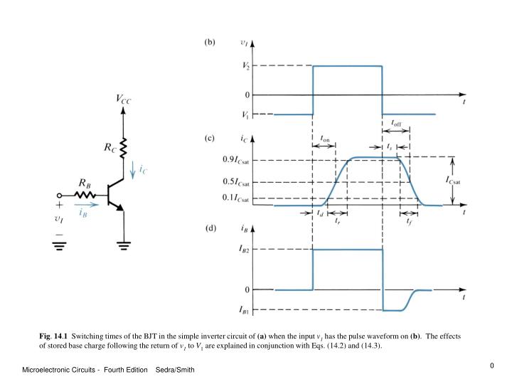
Fig . 14 . 1 Switching times of the BJT in the simple inverter circuit of (a) when the input v 1 has the pulse waveform on (b) . The effects of stored base charge following the return of v 1 to V 1 are explained in conjunction with Eqs. (14.2) and (14.3).

E N D
Fig. 14.1 Switching times of the BJT in the simple inverter circuit of (a) when the input v1 has the pulse waveform on (b). The effects of stored base charge following the return of v1 to V1 are explained in conjunction with Eqs. (14.2) and (14.3). Microelectronic Circuits - Fourth Edition Sedra/Smith
Fig. 14.20 Analysis of the TTL gate with the input high. The circled numbers indicate the order of the analysis steps. Microelectronic Circuits - Fourth Edition Sedra/Smith
Fig. 14.22 Analysis of the TTL gate when the input is low. The circled numbers indicate the order of the analysis steps. Microelectronic Circuits - Fourth Edition Sedra/Smith
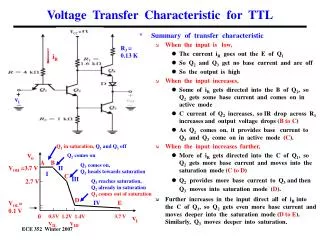
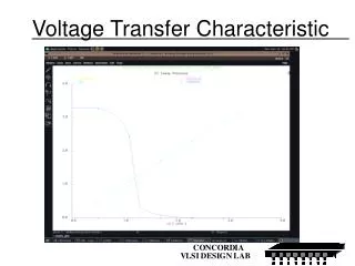
Fig. 14.23 The TTL gate and its voltage transfer characteristic. Microelectronic Circuits - Fourth Edition Sedra/Smith
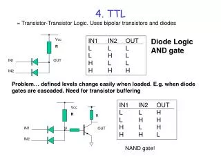
Fig. 14.24 The TTL NAND gate. Microelectronic Circuits - Fourth Edition Sedra/Smith
Fig. 14.25 Structure of the multiemitter transistor Q1. Microelectronic Circuits - Fourth Edition Sedra/Smith
Fig. 14.28 A Schottky TTL (known as STTL) NAND gate. Microelectronic Circuits - Fourth Edition Sedra/Smith
Fig. 14.33 Basic gate circuit of the ECL 10K family. Microelectronic Circuits - Fourth Edition Sedra/Smith
Fig. 14.35 Simplified version of the ECL gate for the purpose of finding transfer characteristics. Microelectronic Circuits - Fourth Edition Sedra/Smith
Fig. 14.36 The OR transfer characteristic vOR versus v1, for the circuit in Fig.14.35. Microelectronic Circuits - Fourth Edition Sedra/Smith
Fig. 14.38 The NOR transfer characteristic, vNOR versus v1, for the circuit in Fig.14.35. Microelectronic Circuits - Fourth Edition Sedra/Smith
Fig. 14.44 Development of the BiCMOS inverter circuit: (a) The basic concept is to use an additional bipolar transistor to increase the output current drive of each QN and QP of the CMOS inverter; (b) the circuit in (a) can be thought of as utilizing these composite devices; (c) to reduce the turn-off times of Q1 and Q2, “bleeder resistors” R1 and R2 are added; (d) implementation of the circuit in (e) using NMOS transistors to realize the resistors; (e) an improved version of the circuit in (c) obtained the lower end of R1 to the output mode. Microelectronic Circuits - Fourth Edition Sedra/Smith