Download

1 / 8
90 likes | 315 Views
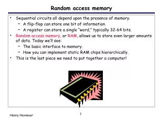
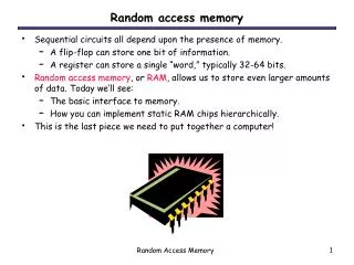
Magnetic tunnel junctions for magnetic random access memory applications M. Guth), G. Schmerber, A. Dinia France 2002. Advantage MRAM have a longevity because of the very important number of reader/write cycles that they can bear.

E N D
Magnetic tunnel junctions for magnetic random access memory applications M. Guth), G. Schmerber, A. Dinia France 2002
Advantage MRAM have a longevity because of the very important number of reader/write cycles that they can bear. ( The write time is not clearly determined; it is reasonable that this time will be lower than 10 ns for addressing bit-memory. ) The commercial memories are in a constant competition for reducing bit memory size and increasing density. ( MRAM can satisfy this target because of the bit-memory matrix addressing structure. ) Power consumption is 1 to 2 times lower than the traditional DRAM memories.
Comparison of a number of characteristics for different Random Access Memories
These two states will constitute the two binary states in MRAM devices.
MRAM’s matrix of MTJ cells and the magnetic field induced by the current flow in a bit line or a word line.
barrier ( aluminum oxide ) most commonly used Oxide has a high gap value and the resistance increases quickly by reducing the junction size, and will give resistance values not compatible with electronic devices.
Fe 4nm / Cu 10nm / Ru 3nm CoFe1nm ZnS2nm CoFe 1.8nm/Ru 0.8nm/CoFe 3nm (AAF) buffer layer Fe6nm/Cu30nm Si substrate
I–V measurement for the 10× 10 mm2 patterned junction composed of Fe 6 nm Cu 30 nm CoFe 1.8 nm Ru 0.8 nm CoFe 3 nm ZnS 2 nm CoFe 1 nmFe 4 nm Cu 10nm Ru 3nm performed at room temperature. Circles correspond to the measured data and the full line corresponds to Brinkman's fit. The inset represents the dynamic conductance (d I/dV) from the I–V measurement at room temperature for parallel (gray line) and ant parallel (black line) orientation.